

Why Multi-Layer PCB Architecture Improves Reliability in SSDs
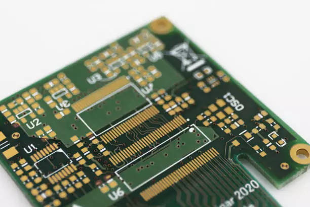
Solid-state drives (SSDs) require high-speed, reliable connections. Modern storage systems depend on stable signal paths and robust thermal performance. A poorly printed circuit board can cause data loss, latency, or failure. A multi-layer PCB architecture addresses these challenges by providing multiple conductive layers, improving signal integrity, and enhancing power distribution. Let’s explore how multi-layer designs improve reliability in SSDs.
Enhanced signal integrity reduces errors
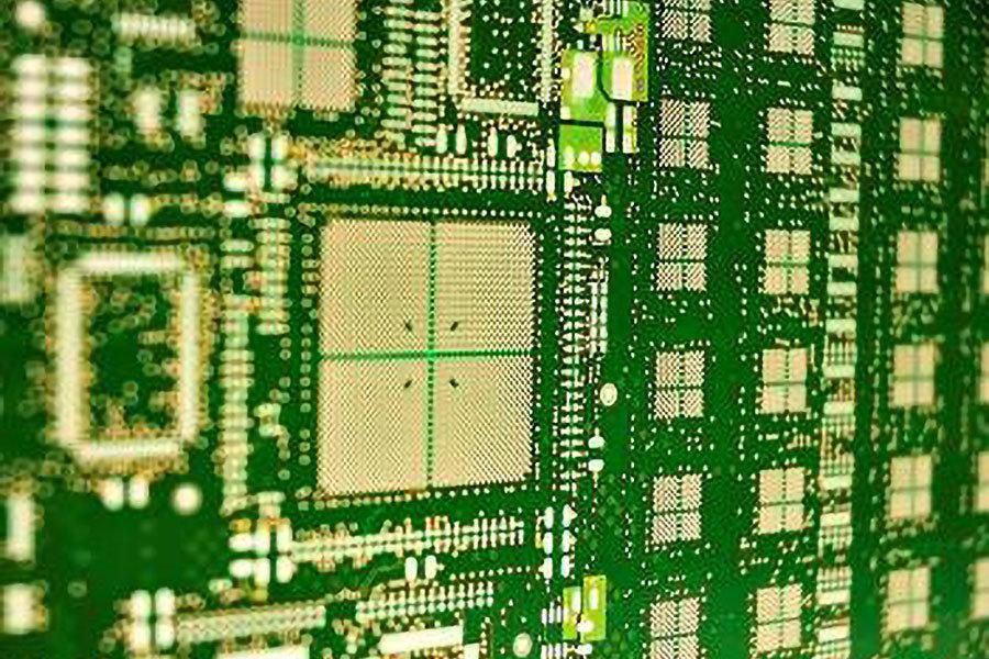
High-speed signals in SSDs are sensitive to interference. Crosstalk or impedance mismatch can degrade performance. A multi-layer PCB allows signal layers to be separated by dedicated ground or power planes. Moreover, controlled impedance reduces reflections and noise. As a result, data travels more reliably across the SSD PCB. Improved signal integrity lowers read/write errors and enhances overall drive reliability. Designers prioritize multi-layer designs for consistent performance.
Better power distribution supports stability
SSDs require stable voltage levels for memory and controllers. Single-layer boards may cause voltage drops during peak loads. A multi-layer PCB architecture distributes power more evenly across its layers. Additionally, power planes reduce electrical resistance and heat generation. Consequently, components maintain operational stability even under heavy workloads. A stable power supply reduces thermal stress, extending component life. Therefore, multi-layer boards enhance reliability and performance in SSD PCB design.
Thermal management prevents overheating
Heat affects the longevity and data integrity of SSDs. Multi-layer PCB structures improve thermal conduction through internal copper layers. Heat spreads across planes rather than concentrating near components. Moreover, vias and thermal pads transfer heat to outer layers and heat sinks efficiently. This reduces hotspots and prevents performance throttling. Better thermal management directly improves reliability, especially in high-capacity SSD PCB systems. Multi-layer boards handle heat challenges effectively.
Compact design enables high-density layouts.
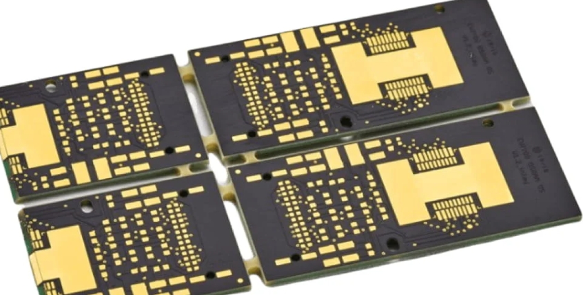
Modern SSDs are compact yet powerful. Single-layer boards cannot support high component density without causing routing conflicts. A multi-layer PCB enables designers to place traces vertically across layers, allowing memory chips, controllers, and passive components to be designed to fit into smaller form factors. Compact layouts also reduce trace lengths, improving signal speed. This is critical for high-performance SSD PCB modules. Multi-layer designs enable denser, faster, and more reliable storage devices.
Reduced electromagnetic interference (EMI)
Electromagnetic interference can corrupt data in high-speed SSDs. Multi-layer PCB architecture mitigates EMI by providing dedicated ground and shielding layers. Moreover, differential pairs and decoupling capacitors are easier to implement across multiple layers. Consequently, signal distortion and noise are minimized. EMI reduction ensures consistent data transmission and prolongs device life. Designers rely on multi-layer boards to control electromagnetic effects in SSD PCB designs.

Improved mechanical strength
Physical durability is crucial in both portable and enterprise SSDs. Single-layer PCBs are more prone to bending or warping. Multi-layer PCBs construction increases rigidity due to stacked copper and substrate layers. Additionally, it reduces the risk of delamination under thermal cycling. As a result, SSDs maintain electrical connections even under mechanical stress. Reliable physical integrity complements electrical performance in SSD PCB solutions. Multi-layer designs protect both function and structure.
Facilitates advanced features and scalability
Multi-layer boards enable advanced SSD features such as higher memory channels and integrated cache. Designers can implement complex routing and additional components without enlarging the PCB footprint. Moreover, this scalability allows future upgrades in performance or capacity. A multi-layer PCB architecture ensures the board can evolve with changing technological demands. Therefore, manufacturers rely on multi-layer designs to deliver feature-rich, reliable SSD PCB products.
Why does a Multi-layer PCB ensure SSD reliability
Multi-layer PCB architecture enhances SSD reliability by improving signal integrity, power stability, thermal management, and EMI control. It enables compact, durable, and high-performance SSD PCB layouts. Moreover, it supports advanced features and scalability for future storage needs. Manufacturers prioritize multi-layer designs to deliver consistent performance, data integrity, and longevity. For these reasons, a multi-layer PCB is essential for modern SSD reliability.