
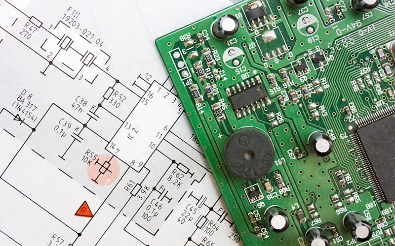
Understanding HDI Stackup Design for High-Frequency Applications
HDI, or High-Density Interconnect, refers to a PCB design approach that incorporates finer lines and spaces, smaller vias, and higher connection pad density. This enables more complex routing and higher component density on a smaller board area. For high-frequency designs, these characteristics are invaluable. They reduce parasitic effects, improve impedance control, and support better thermal management. In short, HDI Stackup Design is not just about fitting more onto a board—it’s about achieving superior electrical performance.
The Importance of Material Selection
Material selection is a cornerstone of practical HDI Stackup Design. The dielectric constant and loss tangent of the substrate material directly influence the quality of signal transmission. In high-frequency applications, materials like FR-4 often fall short due to their higher dielectric losses. Instead, low-loss materials such as Rogers or Isola are preferred. These alternatives offer improved signal fidelity and reduced attenuation, making them ideal for microwave and RF applications.
Moreover, the thermal properties of materials should not be overlooked. High-speed circuits often generate more heat, necessitating substrates that can dissipate thermal energy efficiently. Choosing the right prepreg and core materials ensures mechanical stability and long-term reliability. Ultimately, material selection is not a one-size-fits-all decision; it requires a thorough analysis of both electrical and environmental requirements.
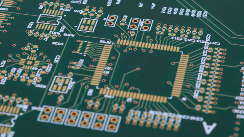
Layer Count and Stackup Configuration
Layer count is a critical factor in HDI Stackup Design. More layers provide greater routing flexibility and improved signal isolation. For high-frequency applications, a balanced layer stack helps maintain consistent impedance and minimizes crosstalk. Designers often use a combination of signal, ground, and power planes to achieve the desired electrical characteristics. This structured approach enhances performance and simplifies EMC compliance.
Stackup configuration also affects manufacturability. Designers must consider the feasibility of drilling microvias and laminating multiple layers to achieve the desired results. Improper stackup can lead to delamination or unreliable via connections. Therefore, collaboration with the PCB manufacturer during the design phase is crucial. By aligning design goals with fabrication capabilities, teams can avoid costly revisions and delays.
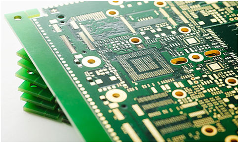
Via Structures and Signal Integrity
Via structures are a defining feature of HDI PCBs. Microvias, blind vias, and buried vias allow designers to create dense interconnects without sacrificing performance. These structures reduce inductance and capacitance, which are vital for maintaining signal integrity in high-frequency circuits. In contrast, traditional through-hole vias can introduce unwanted reflections and signal loss.
Proper placement and optimization can significantly impact board performance. For instance, back-drilling unused via stubs eliminates parasitic resonances. Meanwhile, via-in-pad designs shorten signal paths and minimize impedance discontinuities. When implemented correctly, these strategies enhance signal transmission and ensure the board performs reliably under high-speed conditions.
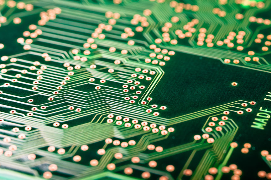
Impedance Control and Signal Layer Management
Controlling impedance is paramount in high-frequency HDI Stackup Design. Impedance mismatches lead to signal reflections, increased jitter, and data errors. Designers must carefully manage trace width, spacing, and dielectric thickness to achieve target impedance values. Tools such as field solvers and simulation software are often used to validate designs before fabrication.
Equally important is the strategic placement of signal layers. High-frequency signals benefit from routing adjacent to continuous ground planes. This setup minimizes loop area and electromagnetic emissions. Alternating signal and ground layers also reduces the risk of crosstalk between adjacent traces. Together, these practices contribute to a clean signal environment and robust system performance.
Power Distribution and Grounding Strategies
Power integrity is as critical as signal integrity in HDI Stackup Design. Poor power distribution can introduce noise and compromise system stability. Implementing dedicated power and ground planes helps maintain a low impedance path for return currents. This reduces voltage drops and improves transient response.
Decoupling capacitors should be strategically placed to filter out noise and stabilize power delivery. Additionally, grounding strategies must support high-frequency return paths. Stitching vias and ground fills can prevent ground bounce and ensure consistent reference planes. These elements, though often overlooked, are fundamental to achieving a reliable high-frequency design.
Thermal Management and Reliability
Thermal management becomes increasingly crucial as device speeds and densities rise. HDI Stackup Design must account for effective heat dissipation to prevent component failure. Thermal vias, heat sinks, and metal cores are commonly used to manage heat in high-frequency PCBs. Without adequate thermal planning, localized hotspots can degrade performance or shorten device lifespan.
Reliability is closely tied to thermal performance. Repeated thermal cycling can cause material expansion, leading to mechanical stress and ultimately resulting in failure. Selecting materials with matched coefficients of thermal expansion (CTE) mitigates this risk. Furthermore, robust manufacturing processes and quality assurance protocols ensure long-term durability and consistent board performance.
Design for Manufacturability and Cost Efficiency
Balancing performance and manufacturability is a key challenge in HDI Stackup Design. Overly complex designs may yield exceptional performance but prove difficult or costly to produce. Therefore, designers must consider standard fabrication capabilities and tolerances. Simplifying via structures or optimizing layer counts can reduce costs without compromising essential features.
Cost efficiency also depends on yield rates. Designs that are prone to defects during fabrication lead to higher scrap rates and longer production times. Engaging with manufacturers early in the design process helps identify potential issues and streamline the production process. Ultimately, a practical approach to HDI Stackup Design ensures high-frequency performance while remaining within budget constraints.
Optimizing HDI Stackup Design for the Future
The future of high-frequency electronics depends on advanced design techniques and robust manufacturing practices. HDI stackup design is the backbone of these developments, providing unparalleled electrical performance and layout flexibility. By understanding the interplay between materials, via structures, impedance control, and thermal management, engineers can build more reliable and efficient systems.