
How to Optimize Trace Routing in Rigid-Flex PCB Layouts
Poor routing during the design of rigid-flex PCB can lead to signal integrity issues, mechanical failures, and increased electromagnetic interference. Unlike traditional rigid printed circuit boards (PCBs), rigid-flex boards must work in a dynamic environment. Traces travel through flex and static areas, each with different stress distributions. Improper routing in the flex area may cause cracking or delamination. On the other hand, optimized routing can extend the product’s life and improve its performance.
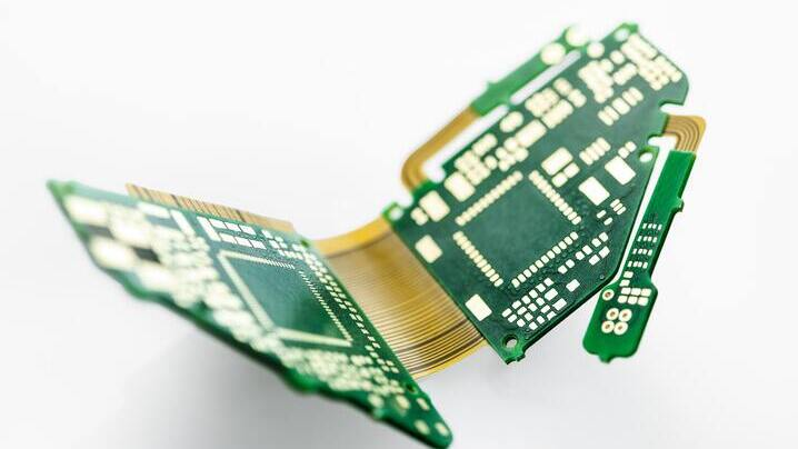
Understand the Anatomy of a Rigid-Flex PCB
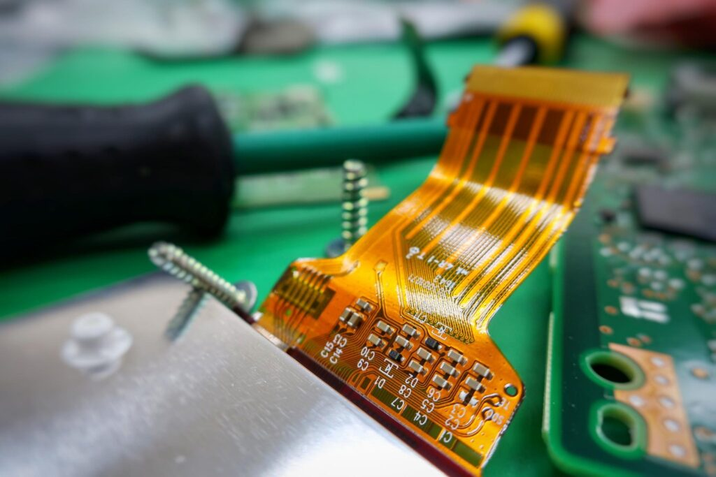
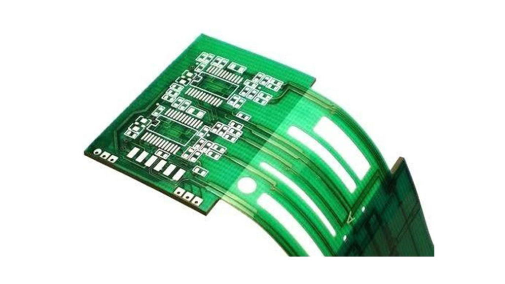
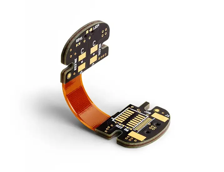
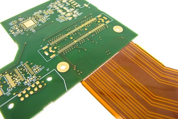
Before diving into routing tactics, you need a clear picture of how a Rigid-Flex PCB is structured. These boards combine rigid FR4 sections with flexible polyimide layers. The rigid areas often house components, while the flex zones accommodate movement or tight-space installation.
Knowing which zones will bend and which remain static helps you determine where to route signals. For instance, power traces should stay out of dynamic flex regions whenever possible. Signal traces, if they must cross a bend, need to follow specific curvature and layering rules. Once you know the physical layout, you can make informed routing decisions that reduce stress and interference.
Use Tear-Drop Pads and Proper Via Placement
Trace-to-pad transitions are hotspots for stress. Tear-drop pads, which provide a gradual width transition between the pad and trace, minimize this risk. They improve mechanical stability and reduce the chance of trace detachment in flex zones.
Additionally, keep vias out of the bending regions. Each via adds stiffness and may introduce failure points during repeated flexing. If you must place a via near a flex region, reinforce it with overlays and ensure it sits within a neutral bend axis. Consistent via placement and design also enhances manufacturability, reducing error rates during assembly.
Apply Consistent Trace Width and Spacing
Signal integrity hinges on impedance consistency. That’s why uniform trace width and spacing are key, especially when routing through flex areas. Don’t forget that the dielectric constants of rigid and flexible substrates differ. Adjust impedance calculations accordingly.
Use wider traces for power delivery, and keep return paths close to signal traces to minimize loop area. Avoid sudden changes in trace direction, as these can create signal reflections. Rounded corners are preferable to sharp angles, especially in flex zones where stress concentration needs to be minimized.
Isolate High-Speed Traces and Reduce Crosstalk
High-speed signals require special attention. Keep them isolated from noisy power or analog lines to prevent interference. Route differential pairs close together and match their lengths precisely to preserve signal integrity.
Use ground shielding or stitching vias to maintain clean signal environments. When routing high-speed traces through the flex section, avoid parallel runs with other signal lines to minimize crosstalk interference. This reduces crosstalk, ensuring the circuit performs as expected, even under dynamic conditions.
Account for Mechanical Stress in Flex Zones
Routing in bendable areas introduces mechanical concerns not present in rigid boards. Always route traces parallel to the bend axis and distribute them evenly along it. This approach minimizes concentrated stress points that lead to failure.
Avoid placing traces at the outer edges of the flex material. These areas stretch the most during bending. Instead, route them through the neutral axis whenever feasible. Also, try to limit the number of layers crossing a flex zone—fewer layers mean less stiffness and a lower risk of delamination.
Balance Electrical Performance and Manufacturability
Great routing design isn’t just about performance—it’s also about making your board buildable. Too-narrow trace widths may boost signal speed but can complicate etching and increase failure rates. Likewise, densely packed traces might save space but compromise inspection and repair accessibility.
Utilise design rule checks (DRC) to align with the manufacturer’s capabilities. Collaborate early with your Rigid-Flex PCBs fabricator to understand their flex material tolerances and stack-up preferences. A realistic layout strikes a balance between performance goals and practical manufacturing needs.
Mastering Trace Routing in Rigid-Flex Layout for Performance and Reliability
Once your layout is ready, put it to the test—Utilise signal integrity simulation tools to validate the performance of your traces. Look for impedance mismatches, timing issues, or signal degradation.
Then, prototype and stress-test the physical board. Bend it, flex it, and monitor how your traces hold up. Don’t hesitate to revise your layout based on test results. Iterative design isn’t a sign of failure—it’s how engineering excellence is achieved.
Mastering Trace Routing in Rigid-Flex Layout for Performance and Reliability
Mastering trace routing in a rigid-flex layout is no easy task. You need to balance mechanical constraints and electrical performance while ensuring the manufacturability and stability of your design. With careful planning and repeated testing, your traces can be built for durability and provide perfect signal transmission.