
How to Implement Multilayer PCBs for High-Frequency Electronics?
Multilayer PCBs (printed circuit boards) are crucial for high-frequency electronics due to their compact design and superior signal integrity. They play a crucial role in applications such as radio frequency communications, high-speed data transmission, and precision measuring instruments. So, how should we construct multilayer PCBs for high-frequency electronics? What key design factors, materials, and manufacturing processes should we consider?
What is a Multilayer PCB
A multilayer PCB is a circuit boards that consist of multiple layers of conductive material separated by insulating layers. These boards are used to support high-density circuits, thereby improving the overall performance of electronic devices. In high-frequency electronics, multilayer PCBs are vital because they provide efficient signal routing while minimising interference and signal loss. The layers in these PCBs are carefully designed and arranged to handle specific high-frequency requirements.
Benefits of Multilayer PCBs in High-Frequency Electronics
The primary benefit of a multilayer PCB is its ability to reduce the overall size of electronic devices. By stacking multiple layers, manufacturers can achieve higher circuit density without increasing the board’s footprint. This is particularly important in high-frequency applications where compactness and space efficiency are critical. Additionally, multilayer PCBs help to improve signal integrity, minimise cross-talk, and reduce electromagnetic interference (EMI), which is vital for high-frequency operations.
Key Design Considerations for Multilayer PCBs
When designing a multilayer PCB for high-frequency electronics, several factors must be considered. First, the number of layers should be determined based on the circuit’s complexity and the need for signal routing. More layers allow for more complex routing, but they also increase manufacturing costs. Second, the impedance of the traces must be controlled to ensure consistent signal transmission. This is particularly crucial in high-frequency designs, where even slight impedance mismatches can cause signal reflections and loss.
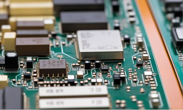
.jpg)
Material Selection for High-Frequency Multilayer PCBs
Selecting the appropriate materials for a multilayer PCB is crucial for high-frequency applications. The most common material used in PCB fabrication is FR4; however, for high-frequency designs, specialised materials such as Rogers, PTFE, or ceramic-based substrates are often preferred. These materials offer low dielectric constants and low loss tangents, which help maintain signal integrity at high frequencies. Selecting the right material minimises signal loss and ensures the PCB operates effectively at the desired frequencies.
Layer Stacking and Routing Strategies
Effective layer stacking is crucial in multilayer PCB designs for high-frequency applications. To minimise signal loss and EMI, signal layers should be placed between ground planes. This arrangement provides shielding, reducing the potential for noise and interference. Additionally, high-frequency signals should be routed with a focus on minimising trace lengths and avoiding sharp bends. Proper routing ensures that signals can travel without distortion or loss, which is vital for the performance of high-frequency electronics.

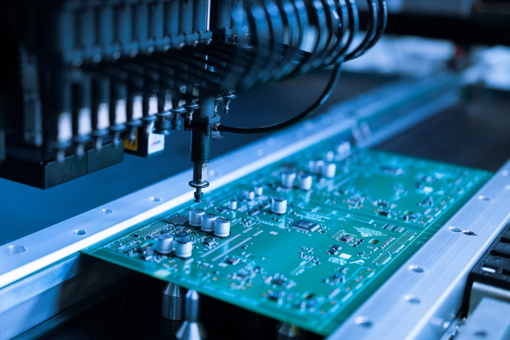
Manufacturing Process of Multilayer PCBs
The manufacturing process for multilayer PCBs involves several steps, including lamination, drilling, and etching. In the lamination process, the conductive and insulating layers are bonded together under heat and pressure. Drilling is used to create vias that connect the different layers of the PCB. For high-frequency electronics, the vias must be precisely drilled to avoid signal loss and impedance variation. Once the layers are assembled, the PCB is etched to create the desired circuit pattern.
Testing and Validation of Multilayer PCB
Testing and validation are crucial for ensuring that multilayer PCBs meet the required standards for high-frequency performance. Electrical testing, such as impedance testing and continuity checks, is used to confirm the integrity of the traces and vias. Additionally, high-frequency testing is necessary to ensure that the PCB can handle the desired frequency range without signal degradation. This testing helps identify any potential issues with the design or manufacturing process before the PCB is used in a final product.
Multilayer PCBs for High-Frequency Electronics
Implementing multilayer PCBs for high-frequency electronics offers several benefits, including compactness, improved signal integrity, and reduced interference. Careful design considerations, including material selection, impedance control, and layer stacking, are crucial for achieving optimal performance. Additionally, a thorough manufacturing process and rigorous testing are necessary to ensure that the PCB meets the high-frequency standards required.