

How SSD PCB Design Impacts Reliability and Performance in Data Center Storage?
Data center operators choose SSDs for their speed and reliability. However, the printed circuit board inside each drive — specifically, the SSD PCB — has a significant impact on both performance and reliability. Design choices on the board change thermal behaviour, signal integrity, power delivery, and testing outcomes. I explain why these choices are essential and cite relevant industry sources where applicable.
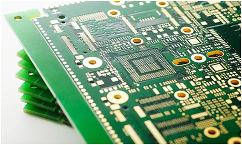
Signal integrity and layout control
High-speed interfaces drive modern SSD performance. For example, PCIe Gen4 pushes signaling near 16 GT/s per lane, which tightens routing tolerances and impedance control. Poor trace geometry or careless via placement can cause jitter and result in retransmissions, negatively impacting throughput. Thus, designers utilize multi-layer boards, matched impedance traces, and meticulous differential pair routing to minimize latency and reduce errors. PCI-SIG details the electrical demands for these higher rates.
Thermal design directly affects endurance.
Heat shortens NAND retention and accelerates cell wear. Engineers commonly use Arrhenius-based reasoning when estimating thermal effects on electronics; higher operating temperatures speed degradation. Laboratory and vendor materials indicate that elevated temperatures can drastically reduce retention and endurance; therefore, practitioners design PCBs to dissipate and remove heat. Real-world guidance and test results on the impact of temperature appear in vendor and technical documents.
Power delivery, PLP, and data integrity
The PCB hosts decoupling capacitors, power rails, and sometimes hardware for power-loss protection (PLP). Clean, well-regulated power reduces bit errors and prevents partial writes during transients. Enterprise SSD vendors and engineering papers describe over-provisioning and PLP circuits as standard practices to mitigate data loss during power events. Good PCB power-plane design and component choice are crucial for both short-term performance and long-term reliability.

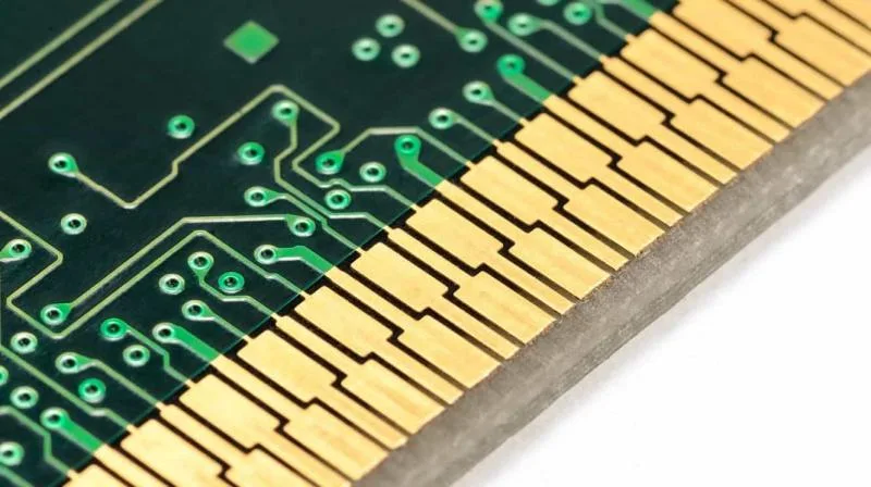
Thermal vias, copper, and materials — practical tactics
A PCB’s layer stack, copper thickness, and thermal via strategy determine how heat moves away from hot ICs. Designers use arrays of thermal vias under heat sources, thicker copper, and heat spreader pads to lower junction temperatures. Academic and industry guides explain via optimization and demonstrate measurable reductions in thermal resistance when vias are applied correctly. These changes let SSD controllers and NAND run cooler under heavy I/O.
Form factor tradeoffs and airflow
Form factors influence board area and cooling options. M.2 modules are compact and fit dense servers, but they offer limited PCB area for thermal features. Conversely, EDSFF and larger form factors permit wider PCBs, more vias, and better heat sinks. Thus, selecting a form factor involves tradeoffs: density versus thermal headroom. Vendors’ product briefs make these tradeoffs explicit.
Testing, JEDEC standards, and validation
Enterprise SSDs undergo endurance, power-cycle, and thermal testing before deployment: industry standards and white papers (including JEDEC-referenced test approaches) guide qualification and endurance measurement. Labs run power-cycling, vibration, and elevated-temperature tests to expose weak PCB design choices. Following these standards helps ensure that a drive survives 24/7 data center workloads.
Future speeds demand tighter PCB engineering
As PCIe generations advance and link rates climb, PCB tolerances shrink. Emerging standards are already pushing designers to consider advanced laminates, tighter stackups, and simulation-led layouts. Also, new NAND types and storage-class memory raise power and thermal requirements. Therefore, forward-looking PCB engineering — backed by simulation and vendor testing — becomes a competitive differentiator.
SSD PCB drives data center outcomes
SSD PCB design shapes real outcomes in data centers. It affects signal integrity, thermal cycling, power stability, and the drive’s performance under stress. For operators, board-level details matter just as much as raw NAND specifications. Therefore, when evaluating drives, ask vendors about their board stackup, thermal via strategy, PLP implementation, and test reports. Those answers directly translate to longer life, fewer failures, and improved performance at scale.