
How Gold Finger PCB Improves Signal Transmission in High-Frequency Boards?
High-frequency boards demand clean, reliable signal paths. Poor contacts or impedance shifts ruin performance. A gold finger PCB addresses these problems at the physical interface. Below, I explain why gold fingers matter, how they affect signal integrity, and what design choices engineers should make.
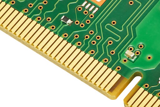
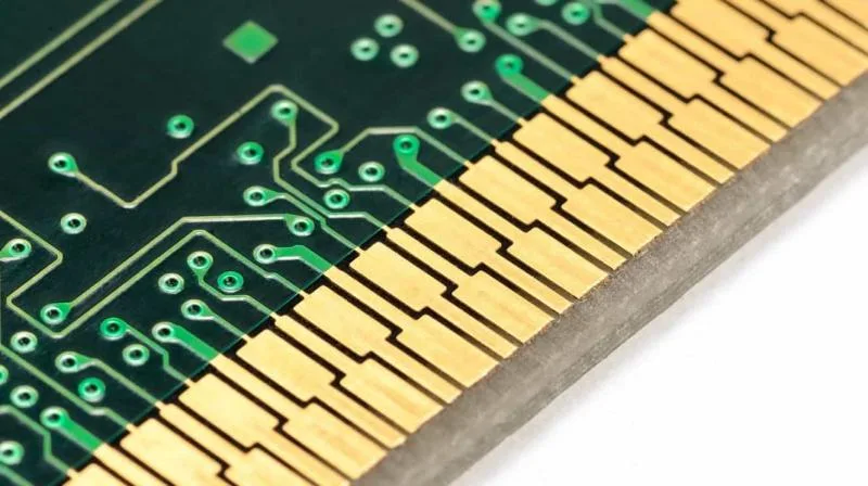
What gold fingers are and why they matter
Gold fingers are the plated edge pads on a PCB. They form the contact surface that mates with connectors or sockets. Because they see repeated insertions, they need both conductivity and wear resistance. Gold plating prevents oxidation and maintains the resistance’s stability over time. As a result, the electrical contact stays reliable. Therefore, devices that rely on high-speed links benefit from gold-fingered connectors. In short, gold fingers reduce the variable that often breaks an otherwise well-designed high-frequency board.
Lower contact resistance and better conductivity
Contact resistance is significant at high frequencies. Even tiny resistance increases create voltage drops and heat. Gold has excellent conductivity and is resistant to corrosion. Thus, it maintains low and stable contact resistance. Moreover, gold’s smooth surface reduces micro-arcing and intermittent contacts. Consequently, the signal sees fewer interruptions and less noise. For signal-critical lines, this steadier contact directly improves transmission quality.
Controlled impedance and smoother transitions
Edges and connectors can create impedance discontinuities. Such mismatches produce reflections. Reflections cause signal distortion, jitter, and bit errors. A well-designed gold finger PCB uses consistent pad geometry to reduce these discontinuities. Additionally, chamfered edges and precise plating thickness help maintain impedance continuity. Therefore, the board transfers energy with fewer reflections. As a result, designers achieve cleaner eye diagrams and higher reliable data rates.
Mechanical durability reduces intermittent loss.
Mechanical factors often cause signal problems. Connectors loosen, friction removes plating, and particles degrade contacts. Gold plating withstands many mating cycles. Moreover, hard gold finishes resist abrasion. Consequently, contact surfaces maintain their shape and conductivity. This durability reduces intermittent connections and packet loss. In mission-critical systems, that reliability prevents unexpected failures and costly downtime.
Surface quality and high-frequency skin effects
At radio frequencies, current flows near the surfaces of conductors. This phenomenon is the skin effect. Therefore, surface finish quality affects effective conductivity. A smooth gold surface lowers surface scattering and skin loss. Additionally, consistent plating avoids micro-roughness that scatters high-frequency currents. Thus, the gold finish helps preserve the signal’s energy where it matters most. For GHz-range signals, this advantage becomes measurable and meaningful.
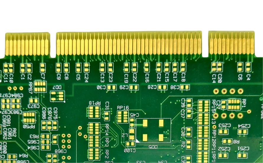
Manufacturing choices that influence performance
Not all gold finishes are created equal. Manufacturers select plating processes based on cost and durability. Hard gold over a nickel underplate is standard for edge fingers that require longevity. Meanwhile, other gold finishes may be suitable for solderability but wear out faster. Engineers must specify the right finish, thickness, and edge profiling. Additionally, plating uniformity and pad flatness are crucial for high-speed contacts. In short, careful manufacturing choices translate into tangible signal benefits on a high-frequency board.
Real-world applications and examples
Gold finger PCBs are commonly used in many high-frequency applications. For example, backplanes, PCIe cards, RF modules, and telecom boards use them to guarantee stable contact. Moreover, test fixtures and development sockets rely on gold for repeatable measurements. In wireless and 5G gear, clean edge connections help maintain low phase noise and low insertion loss. Therefore, designers working with multi-gigabit links often specify gold fingers as a baseline measure of reliability.
Design recommendations for the gold finger PCB
Specify plating and geometry early in the design. First, choose a wear-resistant gold finish for mating surfaces. Next, adjust the control pad width and spacing to match the connector impedance. Also, chamfer the edges to ease insertion and reduce scraping. Furthermore, coordinate with your board house about surface flatness and plating tolerances. Finally, validate the assembly with real-world insertion cycles and signal tests. By following these steps, a gold finger PCB will deliver cleaner transmission, fewer errors, and longer service