
How AI hardware demands are pushing HDI PCB design to new density limits?
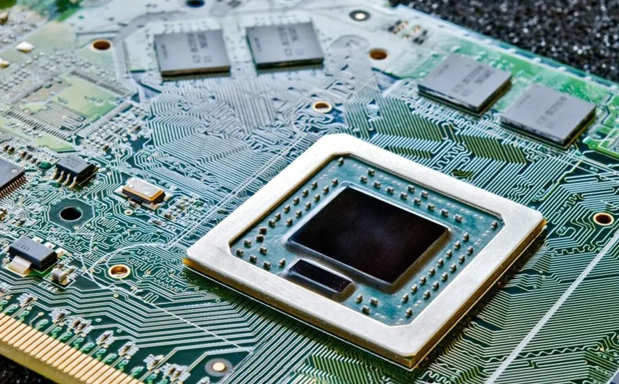
As artificial intelligence continues to evolve rapidly, the demands on hardware are escalating. One critical piece in this equation is the HDI PCB. High-density interconnect printed circuit boards are uniquely positioned to address the challenges presented by AI’s need for speed, capacity, and compactness. AI processors require high-speed data transfer and minimal signal interference—demands that traditional PCB designs can’t meet. To accommodate complex architectures and intense workloads, designers are turning to HDI PCB structures. These boards offer finer lines and spaces, smaller vias, and more connection pads per square inch. This enables compact layouts without sacrificing performance in an era where every nanosecond and millimeter matter. HDI PCBs form the backbone of next-generation AI hardware.
Tight Component Spacing Without Performance Sacrifice
AI hardware demands higher performance in smaller packages. That means tighter spacing between components on the printed circuit board (PCB). Traditional PCBs often fall short in managing heat and maintaining signal integrity in these configurations. HDI PCB technology enables changes that support micro vias, blind/buried vias, and via-in-pad designs, improving thermal performance and reducing electrical noise.
This leads to lower signal loss and faster processing. Additionally, HDI PCBs facilitate shorter routing distances, which enhances electromagnetic compatibility (EMC). By supporting a higher layer count in a smaller footprint, HDI boards enable AI systems to shrink without compromising capability—a key competitive advantage in markets such as robotics, automotive AI, and smart devices.
Enabling Multilayer Complexity for AI Architecture
Modern AI processors utilize multilayer architectures to manage their computational load. This is where HDI PCBs shine. With more routing layers and increased interconnect density, designers can integrate advanced chipsets and memory modules without compromising signal delay or loss. More layers also support parallel processing and multi-core integration, enabling higher AI performance.
Furthermore, HDI technology allows for better impedance control and power distribution. As AI algorithms become more data-intensive, maintaining signal quality and energy efficiency becomes critical. HDI boards help balance these factors through precise design rules and material selection. In essence, HDI PCB design is fueling innovation in AI computing by breaking traditional density limits.
Thermal Management in Compact AI Devices
One of the biggest obstacles in AI hardware development is heat. The more powerful the system, the more heat it generates. HDI PCB designs incorporate thermal vias and copper-filled structures to effectively manage this. These features ensure even heat dissipation, extending component life and maintaining reliable performance under heavy workloads.
Moreover, HDI technology supports advanced thermal interface materials (TIMs) and embedded heat sinks. This makes them ideal for high-performance AI modules in space-constrained environments. Whether in a drone, wearable device, or industrial robot, HDI PCBs help maintain safe operating temperatures without the need for bulky cooling systems. It’s a crucial step toward sustainable, high-efficiency AI hardware.
Reducing Signal Noise and Latency for Real-Time AI
AI doesn’t just need processing power—it needs speed. Real-time applications, such as autonomous driving or real-time data analytics, require ultra-low latency. HDI PCBs are designed with this in mind. By minimizing trace lengths and using high-speed materials, they support rapid signal propagation.
Additionally, HDI PCBs reduce electromagnetic interference (EMI) and crosstalk. Signal noise is the enemy of reliability in AI systems. Features like controlled impedance and ground planes help ensure signal fidelity. The result is a smoother, faster AI response cycle. As demand for real-time performance grows, so too does the role of HDI PCB design.
Design Flexibility Supports Rapid Innovation
AI hardware is evolving rapidly, and product cycles are becoming increasingly shorter. Manufacturers must innovate quickly. HDI PCB design allows for this agility. Designers can prototype, test, and revise complex layouts more efficiently due to the modularity and scalability of HDI technology.
Moreover, HDI PCBs can easily integrate with flexible and rigid-flex substrates. This expands form factor possibilities, enabling the creation of unique product designs tailored to specific AI applications. Whether for AI wearables, edge computing modules, or embedded vision systems, HDI boards offer the design freedom necessary to keep pace with the rapid innovation cycles.
HDI PCBs balance cost and performance
While HDI PCBs may incur a higher upfront cost, they ultimately result in a lower total system cost in the long run. Their compact form reduces housing and material costs. Better performance per square inch translates into fewer boards and less complexity in system integration. This leads to savings in both manufacturing and maintenance.
Additionally, the durability and efficiency of HDI boards result in fewer failures and lower return rates. In mission-critical AI applications, reliability is worth the investment. With fewer reworks and a higher yield rate during production, HDI technology helps optimize the balance between cost and performance.
The Future of HDI PCB in AI Integration
As AI technology continues to grow rapidly, the PCB industry must keep pace with this growth. HDI PCB design is not just keeping up—it’s driving the evolution. By enabling higher interconnect density, improved thermal control, and real-time data flow, HDI boards support the demanding needs of modern AI systems. The demand for AI hardware is pushing HDI PCB design to new density limits. This synergy is unlocking breakthroughs across industries, from competent healthcare to autonomous mobility. HDI is no longer optional—it’s essential for innovation. Companies aiming to lead in AI must prioritize advanced PCB strategies now to remain competitive in the future.