
Heavy Copper PCB cooling and heat dissipation techniques for dense boards
Power-dense electronics place significant stress on printed circuit boards. Standard PCBs often fail to manage heat when designers push them to the limit. In those cases, a board built with thick copper — a heavy copper PCB — wins. Heavy copper dramatically improves thermal conduction. As a result, engineers can build dense boards that stay cooler, run longer, and handle more current. With modern applications such as electric vehicles, renewable energy inverters, and industrial motor controllers, heat management has become critical. This article walks you through real-world cooling and heat-dissipation approaches tailored for dense, high‑power boards.
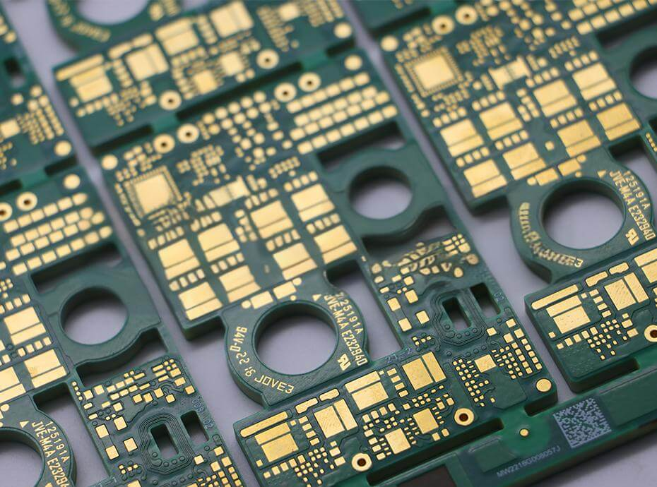
Why Copper Thickness Matters
Copper’s thermal conductivity (about 385 W/m·K) makes it a strong heat conductor. When you increase copper thickness — commonly to 3 oz, 4 oz, or even 6 oz — you enlarge the cross-section for both current and heat flow. That thicker copper spreads heat laterally across planes and traces, reducing hot spots and lowering thermal resistance compared with standard copper layers. Engineers often place heavy copper planes directly under high-current components, such as MOSFETs or power ICs, to act as embedded heat spreaders. This technique can improve a PCB’s thermal performance by up to 30%, depending on power dissipation and layout.
Strategic Use of Thermal Planes and Copper Pour Areas
One core method is to dedicate entire copper planes to power distribution rather than just signal routing. Designers should provide large, contiguous copper areas under or around high‑power components. These planes act as thermal buffers, absorbing and spreading heat over a broad area. In dense boards, such planes often lie in the inner layers, helping manage heat without consuming precious surface space needed for components. By balancing copper distribution across multiple layers, engineers avoid thermal islands, prevent board warping, and maintain electrical performance. In some industrial designs, copper pours can cover up to 50% of the inner layer to optimise heat spread.
Thermal Vias and Vertical Heat Paths
Lateral heat spreading alone is sometimes insufficient, especially in multi-layer or compact designs. Thermal vias — small plated holes — provide vertical pathways for heat to travel from top-layer components to internal planes. Typical via diameters range from 0.30 mm to 0.50 mm, spaced 0.8–1.2 mm apart, depending on current and heat density. Engineers may fill vias with conductive copper or epoxy to further reduce thermal resistance. In high-power applications, a well-designed via array can lower the temperature of top-layer components by 10–20°C under continuous load. Thermal vias are essential on dense boards where space is limited and often complement heat sinks or external cooling solutions.
Embed Copper Slugs or Use Metal-Core Hybrids
For ultra-dense or high-power modules, designers sometimes embed thick copper slugs, colloquially known as “copper coins,” directly into the PCB. Another approach is using metal-core PCB hybrids. Both strategies create low-resistance thermal highways from heat sources to heat sinks or chassis. By embedding copper or using metal cores, designers can lower thermal resistance by 40–60% compared with standard via arrays alone. This method is particularly valuable when external heat sinks are used, allowing the board itself to serve as part of the thermal management system. Some high-current motor control PCBs rely entirely on embedded copper paths to maintain safe operating temperatures.
Thermal Interface Materials and External Cooling
Heavy Copper PCB often reduces the need for large fans or heat sinks, but external cooling may still be necessary. Engineers must select the right thermal interface materials (TIMs) to bridge gaps between PCB copper planes and heat sinks. Thermal pads, greases, or phase-change materials improve heat transfer efficiency on Heavy Copper PCBs. High-performance TIMs maintain stable thermal conductivity during repeated temperature cycling, a crucial requirement for automotive and industrial applications. In extreme designs, liquid cooling or thermoelectric cooling may be used to manage thermal loads exceeding 100 W/cm². However, these approaches are generally reserved for very high-power or compact Heavy Copper PCB systems.
Design Layout and Component Placement Strategies
Even with heavy copper, layout plays a critical role in heat management. Engineers should spread high-dissipation components and avoid clustering multiple hot components in a small area. Leaving copper pour zones around hotspots enhances lateral spreading. High-power modules should be separated from sensitive signal circuits to reduce thermal interference. Using mixed copper-weight layers — heavy copper for power lines, standard copper for signals — allows designers to balance current-carrying capacity with signal integrity. Symmetrical layer stack-ups prevent board warpage and ensure reliability over the product’s life. Real-world designs often see improved reliability and reduced failure rates by applying these layout strategies in combination with heavy copper planes.
Heavy Copper PCB Cooling Strategies for Dense Boards
To build dense, power-heavy boards that stay cool and reliable, designers need more than thick copper — they need thoughtful thermal planning. Using heavy copper planes and pours spreads heat laterally, while thermal vias or embedded slugs channel heat vertically. Proper TIMs and external cooling further enhance performance. Careful component placement and mixed copper layers optimise heat distribution and maintain electrical performance. When these techniques are combined, Heavy Copper PCBs become a thermal backbone for high-power electronics. Boards that follow these principles run cooler, operate longer, and deliver reliable performance even under demanding conditions.