
Design Tips to Maximize Space with Double-Sided PCB
Efficient use of space is one of the biggest challenges in modern electronics. Devices are getting smaller, yet performance demands continue to grow. This is where the Double-Sided PCB plays a key role. By using both sides of the board for routing and components, engineers can achieve compact yet powerful designs. Below are practical design tips to maximize space while maintaining performance.
Plan Layout with Clear Priorities
Good space management starts with planning. Place the most critical components first, such as processors, connectors, or power modules. These parts define the board’s core function. Supporting components, such as resistors and capacitors, should be placed around them in logical clusters.
A well-prioritized layout ensures clean signal paths and efficient use of board area. With a double-sided PCB, you can distribute groups across both sides of the board. This reduces crowding and avoids unnecessary overlaps. For example, a microcontroller and its decoupling capacitors may be placed on top, while related pull-up resistors are positioned on the bottom. Careful planning up front always saves rework later.
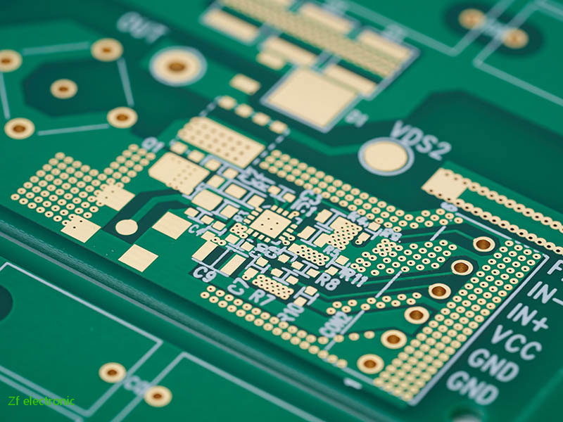
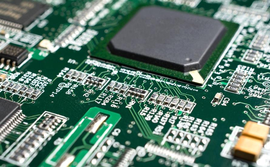
Use Both Layers Strategically
One of the most significant advantages of double-sided PCBs is that it has two surfaces for routing, allowing for more efficient routing. Place high-density circuits on one side and power delivery or ground planes on the other. This approach maintains signal stability and minimizes interference.
You can also place bulky components, such as connectors, on one side and smaller passive components on the other. This balanced strategy prevents congestion. Some designers also separate analog and digital sections by placing them on different layers. Effective use of both layers maximizes every millimeter of available space in a Double-Sided PCB.
Optimize Trace Routing for Efficiency
Routing is often the most time-consuming part of PCB design. For space efficiency, keep traces as short and direct as possible. Use vias to switch between layers instead of running long, winding paths.
Group signals logically. For example, route power lines in one zone and communication signals in another. This not only saves space but also improves performance by reducing crosstalk. Tools like autorouters can help, but manual adjustments often yield cleaner layouts. Efficient routing ensures the Double Sided PCB remains compact without sacrificing clarity.
Leverage Vias and Through-Holes Carefully
Vias are potent tools in two-layer boards. They allow you to move signals between sides and reduce routing complexity. However, each via takes up space and may add resistance.
Use vias only when necessary, and try to align them consistently. Too many vias can crowd the design. Larger through-holes for connectors must also be placed wisely so they don’t interfere with critical traces. A thoughtful balance ensures you keep the board clean and functional. Proper use is a key factor in designing a reliable double-sided PCB.
Balance Thermal Management and Space
Compact boards often face thermal challenges. Placing power components too close together can lead to overheating. Distribute heat-generating parts across both sides for better airflow.
You can also use copper fills or thermal vias to evenly distribute heat. In some cases, adding a small heat sink or aligning hot spots with ventilation slots in the enclosure helps. Balancing space optimization with thermal performance is essential for durability. An efficient thermal design prevents failures and extends the lifespan of your Double-Sided PCB.
Apply Design for Manufacturing Principles
Maximizing space should not compromise manufacturability. Avoid placing tall components directly opposite each other, as this can complicate the soldering process. Maintain consistent clearances to facilitate easier assembly.
Consider automated pick-and-place limitations. Components placed too close to board edges may increase the likelihood of production errors. Also, ensure test points remain accessible for quality checks. Designing with manufacturing in mind ensures cost savings and smooth production of your Double-Sided PCB.
Test and Revise for Best Results
Prototyping is the ultimate test of design decisions. Simulations are helpful, but real boards often reveal space issues. Test the first batch, check thermal behavior, and verify routing clarity.
If necessary, adjust component placement or routing to optimize space utilization. Consider feedback from assembly teams to identify areas of improvement and potential bottlenecks. Iteration is a regular part of the PCB development process. Refining each stage ensures the final Double Sided PCB meets both size and performance goals.
Smart Design Maximizes Double-Sided PCB Potential
Maximizing space with a Double-Sided PCB requires planning, intelligent routing, and practical thermal strategies. When designers balance performance with manufacturability, the result is compact, efficient, and reliable boards. By following these design tips, engineers can fully unlock the potential of double-sided PCBs. The best designs not only save space but also deliver consistent quality in real-world applications.