
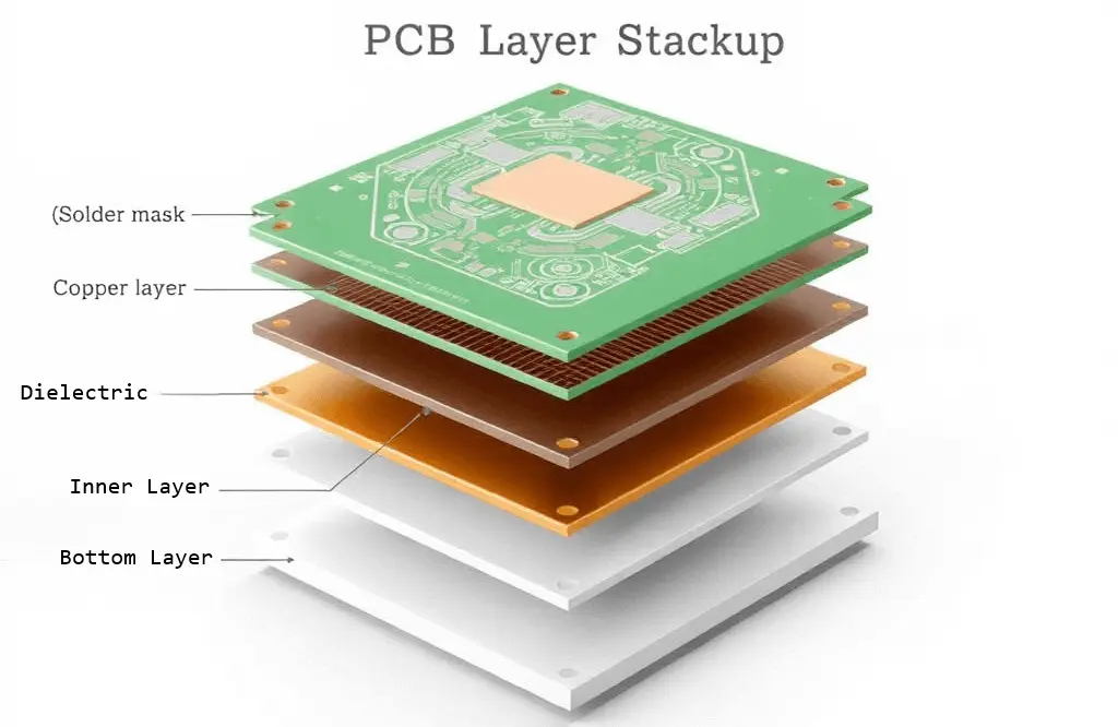
Choosing the Right PCB Stackup for Power Electronics
A robust PCB stackup starts with the appropriate number of layers, copper thickness, and proper layout of ground and power planes. Material selection is also crucial. For high-current designs, such as motor drives or inverters, thick copper PCBs are often preferred due to their ability to handle high currents. They provide a low-impedance power path and improved heat dissipation, allowing all components to operate at a cooler temperature and with greater reliability.
The Impact of Stackup Structure on Thermal Management
Your PCB stackup directly impacts how effectively your board dissipates heat. Multi-layer designs with dedicated thermal vias, thick copper layers, and embedded heat sinks are commonly used to guide thermal flow. Choosing the right materials also affects heat resistance and breakdown voltage.
Designers often opt for heavy copper PCB solutions for enhanced thermal efficiency. The extra copper mass distributes heat more evenly, reducing hotspots and thermal cycling stress. When paired with ceramic-filled or high-Tg laminates, your thermal profile improves significantly. It’s not just about survival—it’s about sustained, peak performance.
Signal Integrity in High-Power Environments
Signal integrity isn’t only a concern for high-speed digital boards. Power electronics are prone to noisy environments, and a poor stackup can exacerbate this issue. Impedance mismatches, ground bounce, and EMI can all disrupt functionality. Innovative stackup strategies help reduce coupling and noise.
You want tightly coupled ground and power planes, solid return paths, and minimal via transitions. Materials with consistent dielectric constants also make a difference. The use of a Heavy Copper PCB architecture further improves low-inductance pathways, which is crucial when working with fast-switching devices. Every bit of interference you eliminate translates into greater efficiency and reliability.
Mechanical Stability and Reliability
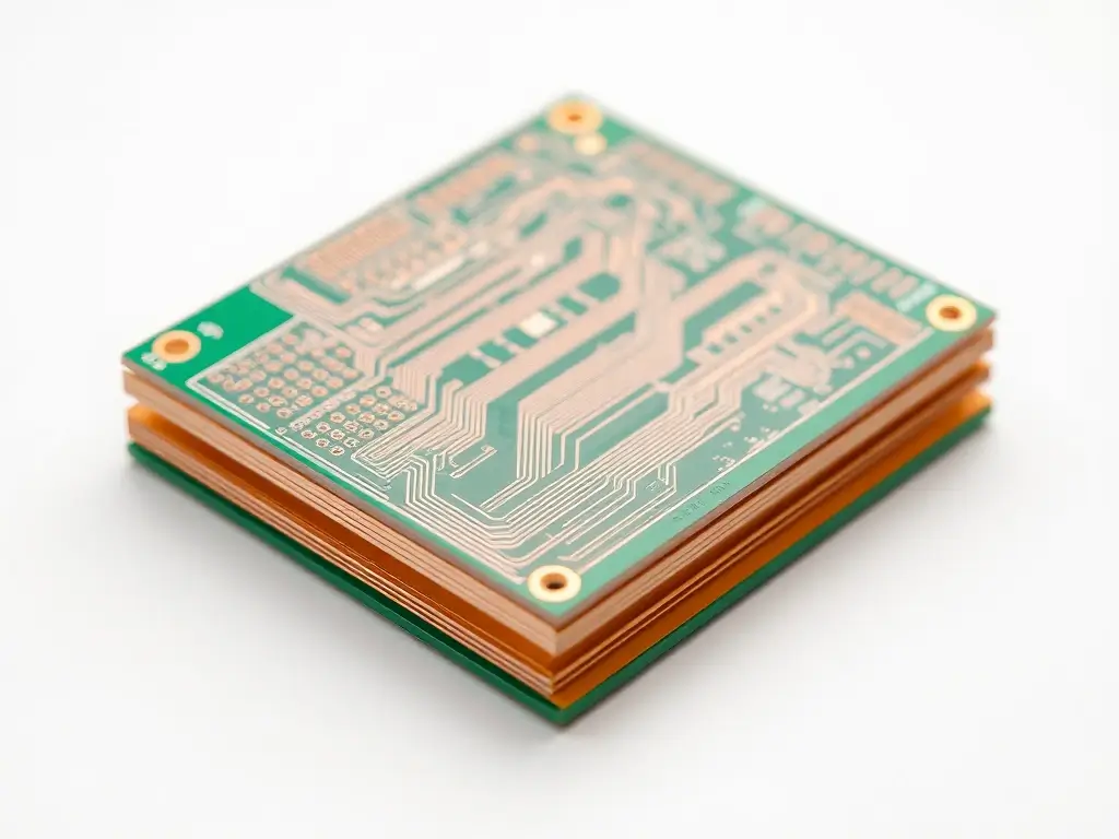
Mechanical durability is often overlooked until something fails. Power electronics are subject to mechanical stresses from thermal expansion, vibration, and external forces. A proper PCB stackup mitigates these risks by distributing stress more evenly across layers and interfaces. This reduces warping, delamination, and fracture.
For rugged environments, Heavy Copper PCB configurations combined with thicker dielectric cores are commonly used. The overall stack becomes more rigid, resisting flex and fatigue. You can even integrate embedded passives or co-fired ceramics for extra mechanical integrity. A stable board means fewer field failures and longer operational life.
.jpg)
Manufacturability and Cost Considerations
Great designs still need to be practical. PCB stackup decisions affect not only performance, but also how easily and affordably the board can be manufactured. Certain stackups require specialized fabrication processes, increasing cost and lead time. Early collaboration with your PCB manufacturer can prevent surprises down the line.
Balancing performance with manufacturability may involve selecting a slightly less complex stackup or utilizing standard copper weights where feasible. However, Heavy Copper PCB designs are worth the premium in high-current scenarios. And if you’re implementing customized warehousing solutions for supply chain flow, predictable stackup choices make inventory planning and fulfillment much smoother.
Electrical Isolation and Creepage Management
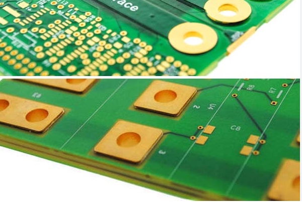
High-voltage circuits require adequate insulation and spacing between conductive elements. A poorly planned stackup can lead to creepage, arcing, or catastrophic failures. Safety standards, such as IPC-2221, provide guidelines; however, every application has its unique nuances.
Designing with staggered layers, offset vias, and reinforced dielectric spacing can significantly improve safety margins. You should also consider conformal coatings and barrier layers where needed. For high-voltage use cases, Heavy Copper PCB layers offer more robustness, reducing failure risk. Plus, stackups that follow logical, repeatable patterns are easier to inspect and verify during production.
Design Tools and Simulation Best Practices
Stackup design isn’t guesswork—not anymore. Simulation tools let you model impedance, heat dissipation, EMI behavior, and structural stress. These tools help refine your stackup before you commit to fabrication. You can virtually test layer combinations and optimize for performance across a range of temperature and voltage extremes.
Utilize software such as Ansys, Altium Designer, or Cadence to simulate power distribution networks and create thermal maps. Especially for Heavy Copper PCB projects, simulations ensure you’re not overdesigning (or under-designing). Combined with customized warehousing solutions for logistics planning, early validation through simulation leads to better design cycles and less scrap.
Why the Right PCB Stackup Matters in Power Electronics
Selecting the correct PCB stackup is essential for the proper operation of electronic components. Leverage intelligent simulation, reliable materials, and proven architectures, such as thick copper PCB design, to meet demanding requirements. Combined with thoughtful logistics planning and customized warehousing solutions, your designs prioritize not only performance but also production, scalability, and long-term success.