
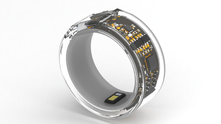
Wearable technology continues to develop rapidly, and bright rings have become a major player in the personal device space. Small, versatile, and feature-rich bright rings offer users a combination of fashion and utility. At the heart of these devices is the smart ring flex PCB, which enables these rings to operate efficiently in a tiny […]
Set-top box PCBs play a crucial role in modern entertainment systems, ensuring high-quality signal reception and output. They enable users to access digital television, cable TV, satellite channels, and streaming services. The PCB, a key component inside a set-top box, is responsible for routing electrical signals and facilitating smooth communication between components such as processors, […]
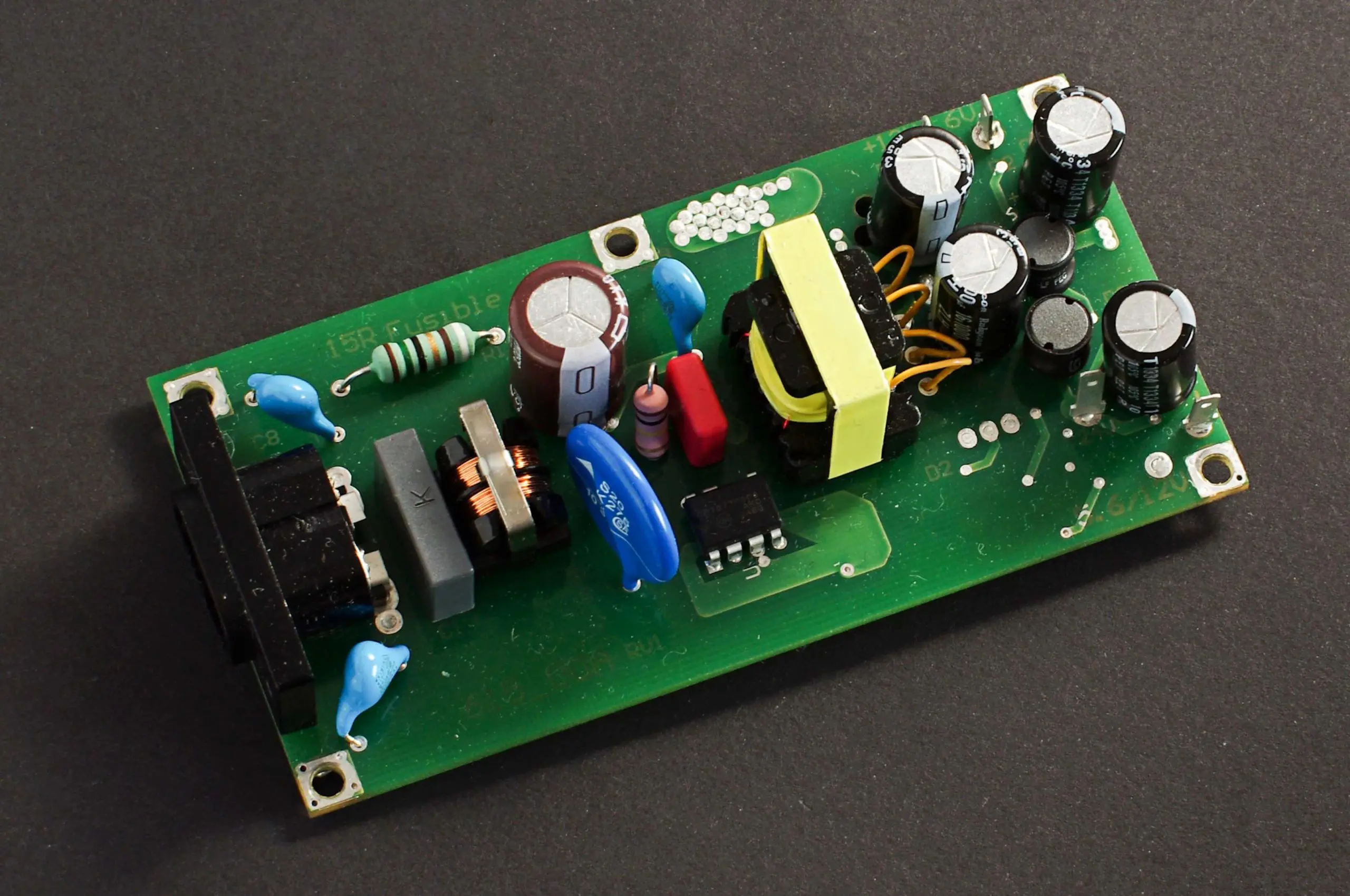
Power supply PCB is an integral component in industrial electronics, providing a crucial link between the electrical supply and electronic systems. Whether regulating voltage, converting current, or distributing power, these PCBs ensure electronic devices operate efficiently and reliably. This article explores the key applications of power supply PCBs in industrial electronics, highlighting their versatility and […]
Double sided PCB, a cornerstone of modern electronics, offer unparalleled flexibility and efficiency in circuit design. By allowing components to be mounted on both sides, these PCBs maximize space and enhance the device’s overall functionality. This blog post will delve into the mounting processes, techniques, and benefits of Double Sided PCBs, equipping you with the knowledge […]
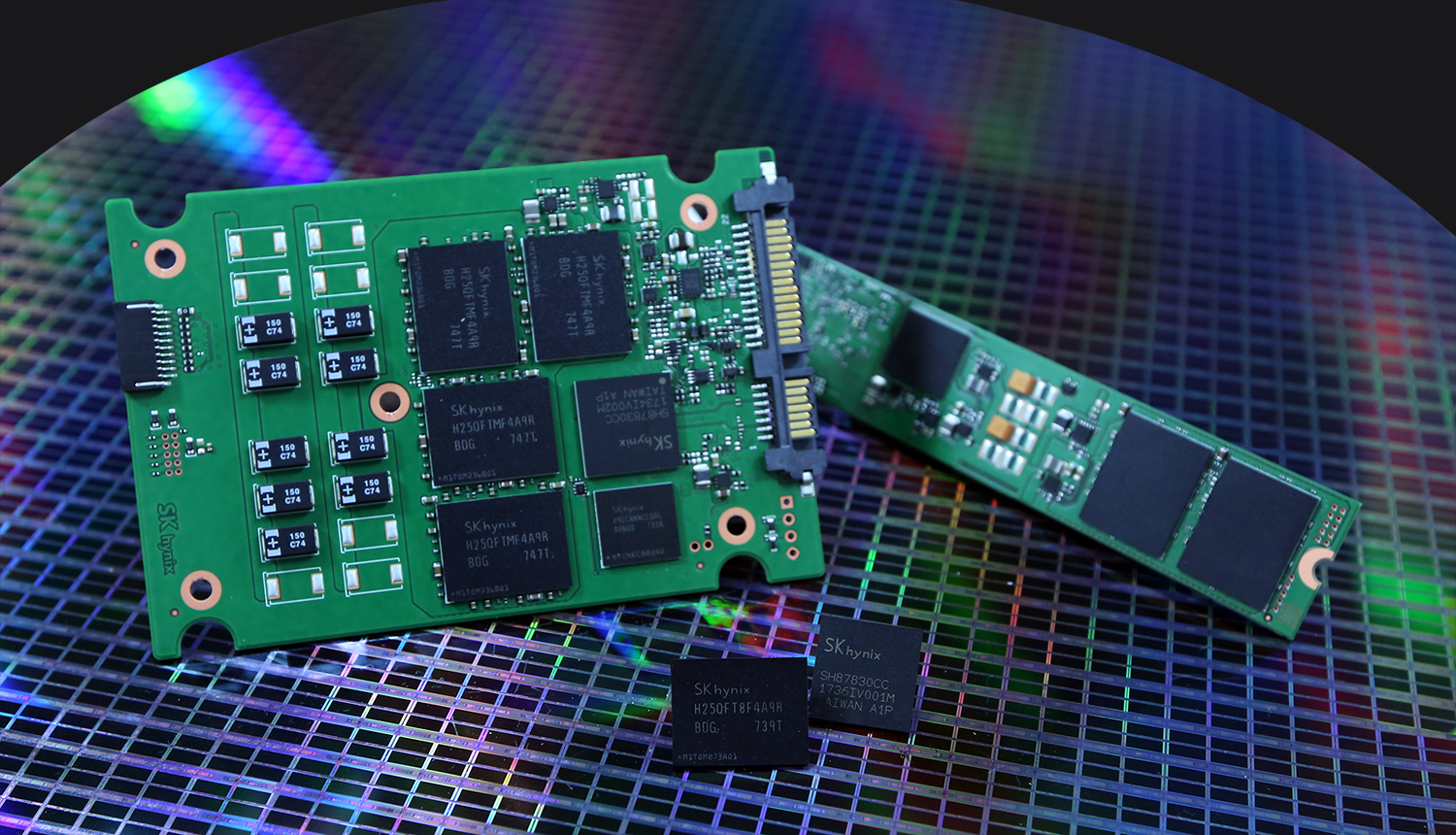
Solid-state drives are essential components in modern computing, providing fast data access and low power consumption. Among the various PCB types used in SSDs, 6-layer SSD PCBs stand out for their ability to offer advanced features, support high-speed data transfer, and ensure optimal performance. Specific materials are needed to build 6-layer SSD PCBs to achieve […]
Printed Circuit Boards are essential components that provide the physical foundation for electronic circuits. The Gold Finger PCB has earned a reputation for superior functionality and reliability among the various types of PCBs available. This blog post explores the advantages of using Gold Finger PCBs, particularly in high-performance and demanding applications. Gold Finger PCB Introduction […]
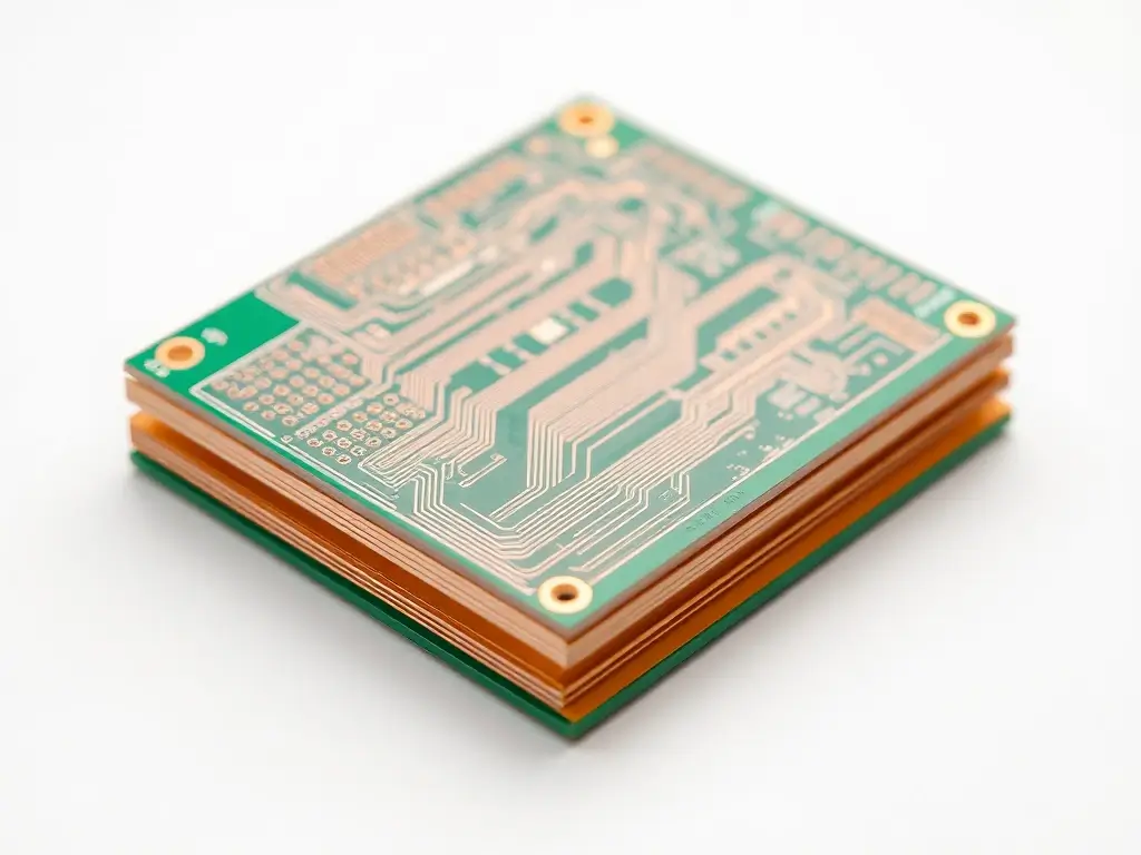
In today’s rapidly evolving electronics world, as the demand for advanced and miniaturized electronic products grows, the custom multi-layer PCB is also increasing. Custom multi-layer PCBs offer a variety of benefits, including improved performance, greater cost-effectiveness, and the ability to meet specific design requirements for different applications. Custom multilayer designs enable engineers and manufacturers to achieve the […]
When considering the purchase of a Solid State Drive, many users are concerned about the compatibility of the SSD PCB with various motherboard architectures. SSDs are now essential for fast data access and reliable storage, making it crucial for consumers to know whether the SSD they choose will integrate seamlessly into their existing system. The […]
Power distribution systems are critical to the performance and reliability of electronic devices, machinery, and networks. As industry demands more energy-efficient systems, the materials used in power distribution components must evolve. Heavy copper PCB is a crucial innovation in this regard, with thicker copper layers that can handle high currents while preventing heat buildup—two critical […]
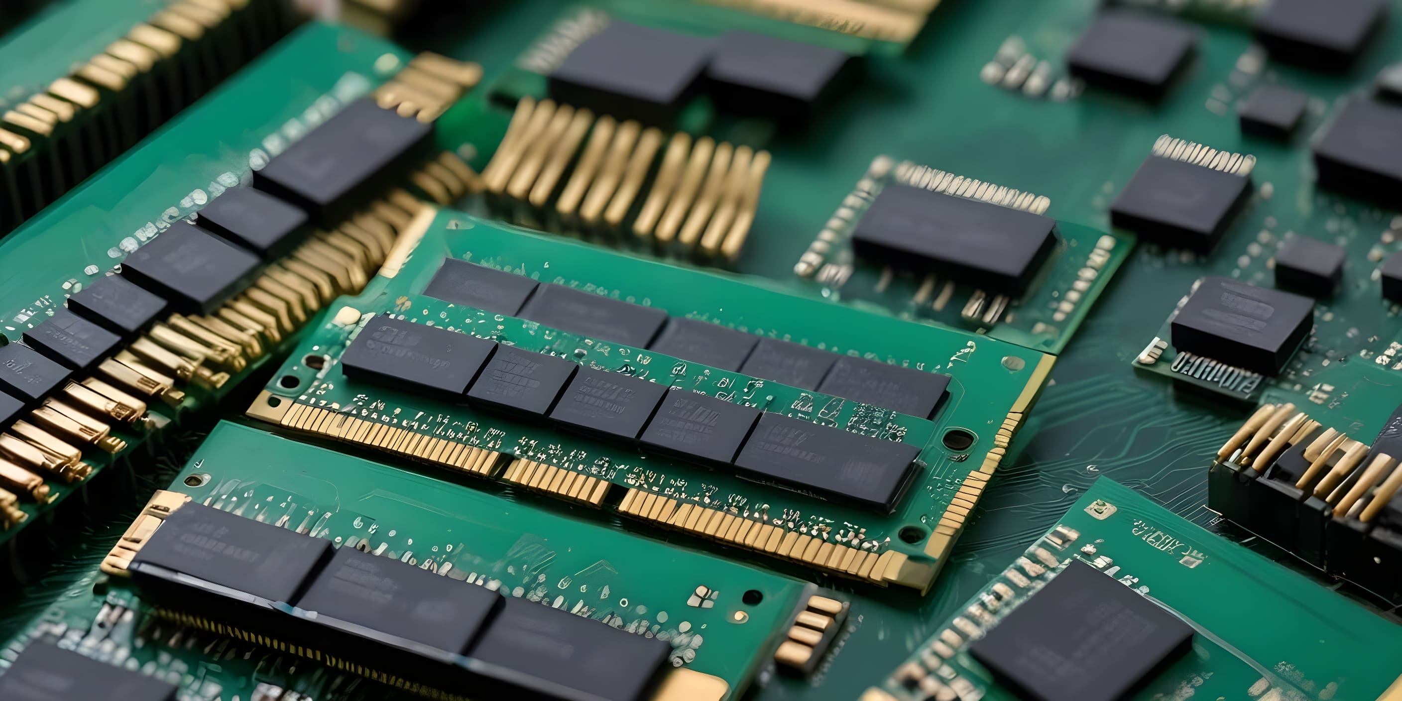
As the demand for faster, more efficient, and more compact storage solutions continues to grow, manufacturers are constantly innovating in the design of printed circuit boards. An 8-layer SSD PCB is a prime example of how technological advancements have enabled the integration of power and signal layers to improve performance and reliability. This blog post […]