
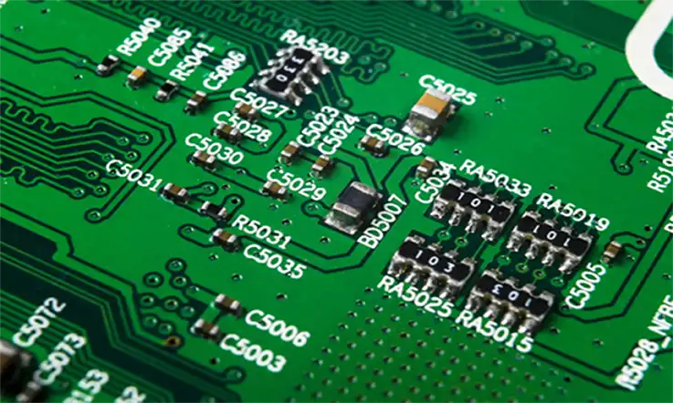
How HDI PCB Improves Connectivity in IoT Smart Appliances?
IoT smart appliances demand reliable links. They also require compact electronics and low power. Consequently, board design now defines device performance. High-density interconnect (HDI) PCBs answer many of those needs. They pack traces, vias, and components more tightly. As a result, signal integrity and RF performance improve. Moreover, HDI PCB lets designers place radios and sensors closer to the processing core. That reduces losses and latency. HDI helps devices stay connected, responsive, and efficient in real-world use.
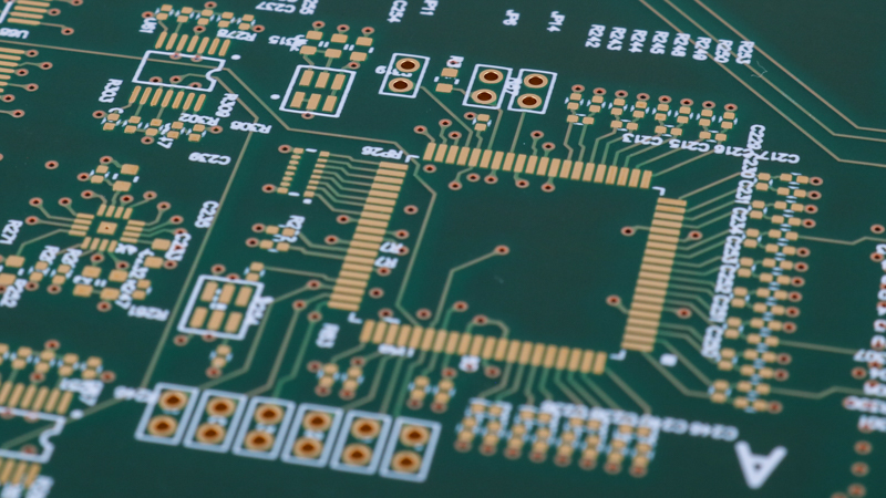
Higher Trace Density Enables Complex Routing
HDI technology uses microvias and finer traces. Therefore, designers route signals with fewer compromises. As a result, you avoid long detours and awkward jumpers. Consequently, you preserve signal strength and timing. Additionally, narrower traces reduce board area while maintaining clean routing.
Furthermore, buried and blind vias provide free surface area for components. Thus, antennas and RF chains are placed optimally. Ultimately, denser routing directly benefits the radio and digital domains in IoT appliances.
Shorter Signal Paths Improve RF and Data Integrity
Short signal paths cut parasitic inductance and capacitance. Therefore, RF front-ends work closer to their intended specs. As a result, you see a better range and fewer retransmissions. Additionally, shorter paths reduce the latency between sensors and controllers. Moreover, careful impedance matching on HDI boards lowers reflections. Consequently, receivers see cleaner waveforms and higher SNR. Thus, HDI PCBs designs help radios meet coexistence and regulatory targets more reliably.
Improved Power Distribution and Thermal Management
HDI stackups allow solid power planes and dense via stitching. Therefore, you achieve a lower voltage drop across the board. As a result, sensitive RF amplifiers and SoCs receive steadier power. Additionally, thermal vias and copper pours help dissipate heat away from hotspots. Consequently, chips run cooler and maintain calibration longer. Moreover, stable power reduces phase noise and gain drift in RF stages. Thus, good HDI power design directly supports long-term connectivity and device longevity.
Smaller Form Factor and Better Antenna Placement
HDI boards free up space for antennas and sensors. Therefore, engineers can place antennas away from noisy components. As a result, antenna efficiency rises and detuning falls. Additionally, compact boards enable manufacturers to design sleeker housings. Consequently, consumers get smaller, more attractive appliances without sacrificing range. Additionally, embedding passive components saves board space and reduces the number of signal paths. Thus, HDI PCBs enable both form-factor gains and stronger wireless performance.
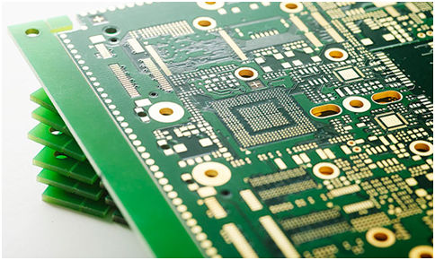
Manufacturing Quality and Reliability
HDI fabrication demands tighter tolerances and better process control. Therefore, choose manufacturers with proven HDI experience. They will control microvia formation, drill registration, and plating uniformity. Additionally, they will adhere to IPC standards and conduct controlled impedance tests. Consequently, finished boards show consistent electrical behavior across batches. Moreover, robust QA catches delamination, voids, and plating defects early. Thus, production reliability translates into predictable field connectivity for end users.
Design Flexibility That Speeds Time to Market
HDI lets designers consolidate functions and reduce layers in many cases. Therefore, you can prototype more quickly and iterate faster. Additionally, design-for-manufacture (DFM) practices help reduce late-stage surprises. Consequently, teams shorten their validation cycles and deploy updates more quickly. Also, HDI supports component-in-pad and embedded passives when appropriate. Thus, the design team can optimize the BOM and assembly steps, which lowers costs and speeds up delivery.
Testing, Certification, and Field Validation
HDI enhances electrical performance, but testing remains crucial. Therefore, run controlled impedance checks, RF sweeps, and thermal cycling. Additionally, perform OTA range and coexistence tests in real-world environments. Consequently, you validate both lab performance and in-home reliability. Moreover, track failure modes and use telemetry to monitor degradation. Thus, certification and ongoing validation ensure that the HDI PCB supports stable connectivity throughout the product lifecycle.
Final Recommendations for HDI PCB
Start with precise connectivity requirements and a target stackup. Then, specify controlled impedance, microvia size, and material Tg up front. Also, prioritize antenna placement and thermal vias in the layout. Next, select an HDI-friendly contract manufacturer that offers IPC and impedance testing capabilities. In addition, run OTA and environmental tests before release. Finally, document DFM rules and plan for firmware-assisted calibration. By following these steps, your IoT smart appliances will benefit from the compact routing, better power integrity, and improved RF behavior that an HDI PCB provides.