
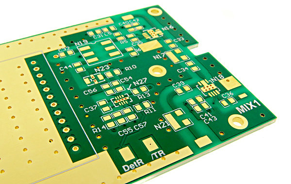
Choosing the Right Dielectric Material for High Frequency PCB with Gold Finger Interfaces
Selecting the appropriate dielectric material is crucial for PCBs, particularly for a high frequency PCB. You need a dielectric material with a stable dielectric constant and a low loss tangent. This is non-negotiable. If the material fails to maintain its electrical properties at high frequencies, signal degradation and electromagnetic interference (EMI) issues can occur. If signal degradation occurs in high-speed interfaces, it not only degrades performance but also compromises the entire board’s functionality.
The Trade-Off Between Dk, Df, and Manufacturability
Procurement teams and engineers often clash in this area. Engineers want the lowest possible dielectric constant (Dk) and dissipation factor (Df). Procurement wants to keep costs down. However, cutting corners on materials in a High-Frequency PCB can lead to headaches later—especially with gold-finger PCB designs.
Choose materials like Rogers, Isola, or Taconic when performance outweighs price. These materials deliver excellent signal control and consistent impedance. If the board layout includes complex routing or tight tolerances near gold fingers, it’s even more critical to ensure the dielectric doesn’t fluctuate under thermal or mechanical stress.
Thermal Management and Stability Concerns
Heat is a silent killer. If your dielectric expands unevenly in response to temperature fluctuations, the impedance can shift, creating signal reflections. That’s a nightmare for high-frequency signals and gold finger PCB edge interfaces.
Look for materials with a low coefficient of thermal expansion (CTE), especially in the Z-axis. PTFE-based materials are excellent, but they can be tricky to fabricate. If your project demands fine-pitch connectors or multi-layer stacks with gold fingers, you’ll need a dielectric that behaves well under both thermal and electrical stress.
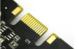
Compatibility with Gold Finger Plating Processes
Gold finger PCBs require ENIG or hard gold plating. Not all dielectric materials play nice with these processes. Some may delaminate or warp during the plating or reflow process. Always cross-check material compatibility with the finishing steps in your stack-up to ensure optimal results.
Also, pay attention to how the dielectric handles chemical exposure during the gold plating process. A stable surface ensures proper adhesion and minimal contamination risk. This isn’t just about electrical performance—it’s also about mechanical reliability.
Material Loss at Higher Frequencies
Some materials look perfect on paper but behave differently in the real world. Lab-tested loss tangent might not reflect performance in your actual PCB configuration. Factors such as board thickness, copper roughness, and surface preparation can all affect high-frequency behaviour.
Use test coupons. Validate performance with prototypes. Especially for gold finger PCB applications, a minor impedance mismatch can create connection failures at the edge interface. Don’t gamble with signal loss—test early and often.
Stack-Up Design Strategy and Dielectric Role
The dielectric doesn’t live in isolation—it’s part of a stack-up. Your layer configuration affects everything from impedance control to cross-talk. In a high-frequency PCB with gold fingers, a poor stack-up will quickly expose weaknesses in your dielectric choice.
Use symmetric stack-ups to balance mechanical stress. Place reference planes near signal layers. Ensure that prepregs and cores are matched for dielectric constant. These minor design tweaks can significantly boost reliability and reduce failure rates in edge-connector designs.
Choosing a Dielectric That Balances Performance and Production Yield
You want performance, but you also wish to yield. Some high-performance dielectrics can be challenging to laminate or drill, particularly when gold finger PCB requirements are involved. Poor drill quality at the connector interface can compromise insertion durability and lead to long-term wear issues.
Talk with your fabricator. Receive feedback on which materials strike a good balance between electrical properties and manufacturability. If your gold fingers require beveling, ensure the material can handle mechanical processes cleanly without micro-cracking.
Selecting the Best Dielectric for High-Frequency PCB with Gold Finger Interfaces
In high-frequency PCB design, dielectric materials aren’t just a background detail; they’re fundamental. And when gold-finger PCB connectors become part of the design, every flaw is magnified. You need a material that offers stable electrical performance, thermal stability, and plating compatibility. The right choice depends on your frequency range, signal type, mechanical design, and manufacturing process. But by asking the right questions and validating material performance early on, you can mitigate risk and improve reliability.