
Why Layer Stackup Is Critical for Successful Rigid-flex PCB Design?
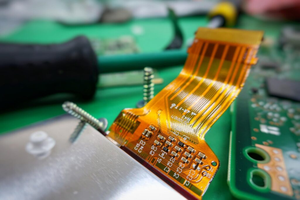
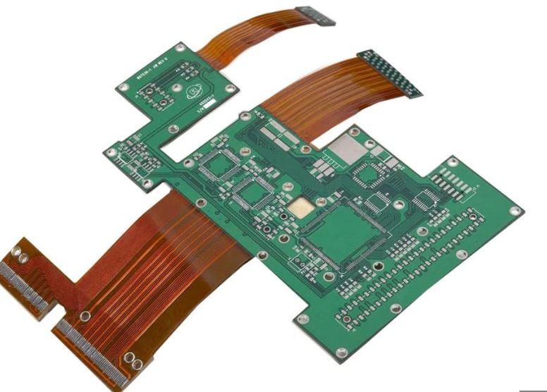
In Rigid-flex PCB design, every decision shapes product performance. Among these, the layer stack-up is especially critical. It determines not just electrical performance but also mechanical durability and manufacturing reliability. Layer stackup refers to the arrangement of conductive and insulating layers within the PCB. For Rigid-flex PCB designs, this process becomes more complex due to the hybrid nature of rigid and flexible sections. A poor stackup can lead to signal integrity issues, mechanical failure, or production delays.
Optimizing Electrical Performance Through Thoughtful Stackup
Electrical performance is a top priority in Rigid-flex PCB design. A proper layer stack-up minimizes impedance variation, reducing risks of signal loss and electromagnetic interference. Each layer’s placement affects how signals travel across the board.
In high-speed designs, controlled impedance is vital. Engineers use specific stack-ups to maintain signal integrity across rigid and flexible sections. Additionally, well-planned stack-ups ensure adequate power delivery and ground returns, preventing voltage drops and noise. Careful attention to electrical parameters within the stackup design provides consistent, high-quality circuit performance throughout the product’s lifecycle.
Mechanical Reliability and Flexibility Balance
Rigid-flex PCB designs must strike a balance between flexibility and mechanical strength. The layer stack-up directly influences this balance. Too many layers in flexible regions can cause cracking or delamination, while too few layers may reduce strength.
Manufacturers optimize stack-ups by strategically positioning flex layers and reinforcement materials. This improves bending tolerance without compromising durability. Furthermore, designers often stagger layers to reduce mechanical stress concentrations. By fine-tuning the layer stack up, engineers can enhance product resilience in applications that require repeated flexing or exposure to challenging environmental conditions.
Thermal Management for Long-Term Stability
Thermal performance is another crucial factor tied to stackup design. Rigid-flex PCB designs often operate in tight spaces with limited airflow. The layer stack-up plays a direct role in heat dissipation and thermal cycling resistance.
By integrating thermal vias, copper pours, and heat-spreading layers into the stack-up, designers can effectively manage hotspots. Additionally, insulating materials with high thermal stability are selected to prevent deformation. Through proper stackup planning, engineers reduce thermal stress on components and connections, ensuring product stability under continuous or high-temperature operation.
Manufacturability and Production Yield Considerations
Layer stack-up choices also impact manufacturability. Complex Rigid-flex PCB designs often require tight tolerances during lamination, drilling, and plating processes. An improper stackup can complicate production or lead to defects.
Manufacturers must assess whether the stackup design aligns with their production capabilities. Using symmetrical layer configurations often improves process control and reduces warpage. Moreover, stacks that simplify drilling and etching minimize the risk of production delays. A design optimized for manufacturability not only increases yield but also reduces costs and turnaround times.
Material Selection and Compliance Factors
Selecting the right materials is inseparable from stackup planning. Each material’s properties, such as dielectric constant, thermal expansion, and flexibility, influence the Rigid-flex PCB’s performance.
Engineers must also consider regulatory compliance, particularly in industries such as aerospace or medical devices. Materials used in the stack must meet fire resistance, chemical durability, and environmental safety standards. Additionally, supply chain availability influences the selection of materials. By aligning material choices with stackup design, companies can produce safe, reliable, and compliant PCBs at scale.
Design for Reliability Testing and Validation
Once the initial stackup is defined, testing becomes essential. Rigid-flex PCB prototypes undergo electrical, mechanical, and thermal stress tests to validate performance under real-world conditions. A poorly optimized stack-up often fails during such evaluations.
Testing protocols often include dynamic flexing, high-temperature exposure, and vibration analysis. Engineers must refine their stackup designs based on test results to eliminate weaknesses. Additionally, reliability validation ensures that the chosen stack up can endure the product’s intended lifecycle without degradation, minimizing warranty risks and field failures.
Why Layer Stackup Matters Most in Rigid-flex PCB Projects
Layer stackup defines the success of every Rigid-flex PCB project. It affects signal integrity, mechanical durability, thermal management, manufacturability, and compliance. A well-engineered stack-up transforms complex designs into high-performance, reliable products