
How SSD PCB Design Affects Storage Performance and Reliability?
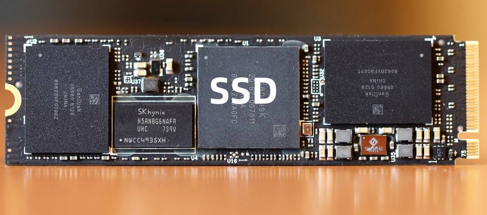
The design of an SSD PCB plays a critical role in determining both the performance and reliability of storage devices. The printed circuit board (PCB) acts as the foundation for all electronic components, including the NAND flash, controller, DRAM cache, and power management systems. Without well-engineered SSD PCBs, even the most advanced memory chips cannot function effectively.
Signal Integrity and Data Transmission Speeds
Signal integrity is one of the most vital aspects of SSD PCB design. Poor signal quality can lead to data errors, latency spikes, and a reduction in overall performance. To ensure clean signals, designers carefully manage trace routing, impedance matching, and grounding to maintain a stable signal path.
High-speed data lines, such as those connecting the controller to NAND flash, require special attention. Techniques such as differential signalling and controlled impedance traces help maintain data integrity. Additionally, minimising crosstalk and electromagnetic interference (EMI) is essential for stable operation. In short, optimising the SSD PCB for signal integrity ensures fast and accurate data transfers.
Power Delivery and Energy Efficiency
Reliable power delivery is another crucial factor in the performance of SSD PCBs. Modern SSDs require precise voltage regulation for components like the controller and DRAM cache. An inadequate power supply can lead to instability, data loss, or a reduced lifespan.
Designers utilise techniques such as multilayer PCB stacking and dedicated power planes to manage power efficiently. Voltage regulators and filtering capacitors stabilise power throughout the board. Moreover, optimising power distribution reduces heat generation, which is vital for energy efficiency. Effective SSD PCBs’ power design improves both performance and long-term reliability.
Thermal Management and Heat Dissipation
Heat management is becoming increasingly crucial in SSD design. Higher speeds and compact sizes generate more heat, which can degrade component performance over time. An SSD PCB with poor thermal management is at risk of overheating and a reduced lifespan.
To combat this, designers use thermal vias, copper pours, and heat spreaders to disperse heat. Proper component placement also enhances airflow and cooling efficiency. Furthermore, some SSDs integrate external heatsinks connected directly to the PCB. These strategies allow the SSD PCBs to maintain optimal temperatures, ensuring stable performance under heavy workloads.

Component Layout and Space Optimisation
Efficient component layout on the SSD PCBs affects both functionality and manufacturability. A well-structured PCB minimises signal path lengths, reducing latency and power loss. It also allows for easier assembly and quality control during production.
Designers often use 3D modelling software to optimise the layout before manufacturing. This process helps identify potential conflicts between components and ensures efficient use of board space. Additionally, a careful layout improves structural integrity, reducing the risk of mechanical failure due to physical stress. Ultimately, innovative SSD PCB layouts strike a balance between performance and durability.
Impact of SSD PCB on Data Reliability
Data reliability heavily depends on the quality of the SSD PCB design. Factors like signal noise, voltage fluctuations, and thermal stress can all compromise data integrity. A robust PCB design minimises these risks, protecting stored information.
Error-correction features also benefit from stable PCB designs. Reduced electrical noise helps error correction algorithms work more effectively. Moreover, consistent power delivery prevents sudden data loss during voltage dips or power cycles. In essence, a reliable SSD PCB ensures that stored data remains safe and accessible.
Longevity and Wear Management
The lifespan of an SSD is closely tied to the durability of its PCB. Constant heat cycling, voltage changes, and high-speed operations can stress PCB materials. Without proper design, these stresses can cause long-term degradation or component failure.
Designers select high-quality materials and advanced construction techniques to extend PCB longevity. Reinforced fibreglass, thicker copper layers, and high-temperature solder joints all improve durability. Furthermore, effective SSD PCB design reduces wear on flash memory by ensuring stable operations, thus extending the drive’s usable life.
SSD PCB as the Foundation of Storage Performance and Reliability
The SSD PCB serves as the backbone of storage performance and reliability. Its design directly impacts signal integrity, power delivery, heat management, and data stability. Without a well-optimised SSD PCB, even the fastest memory components cannot perform at their best.