
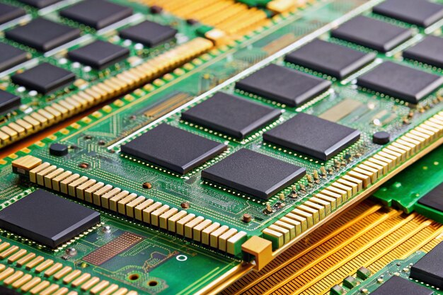
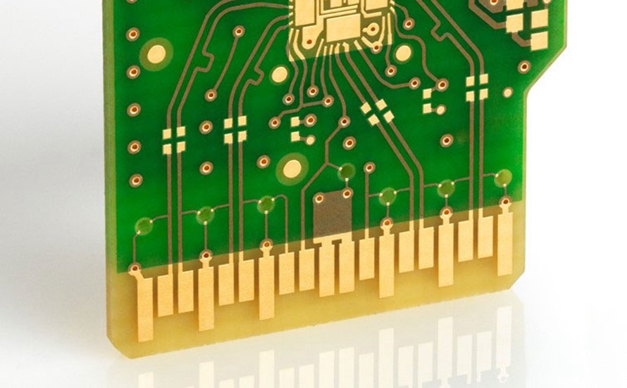
The Role of ENIG vs Hard Gold Plating in Gold Finger PCB Longevity
When it comes to the performance and durability of Gold Finger PCB assemblies, surface plating isn’t just a technical detail—it’s a critical design decision. Engineers and OEMs often face a common choice between ENIG (Electroless Nickel Immersion Gold) and Hard Gold plating. While both serve the same function—protecting the contact edge of PCBs—their characteristics vary significantly, especially in long-term applications.ENIG offers excellent flatness and solderability, making it ideal for specific assembly processes. However, Hard Gold excels in high-wear environments, such as repeated insertions and removals in card-edge connectors. Understanding the strengths and trade-offs of each helps in optimising performance, cost, and longevity.
What ENIG and Hard Gold Are Made Of
To start, it’s essential to break down what each plating type involves. ENIG consists of a dual-layer coating: a nickel layer that provides structural support and a thin gold layer that prevents oxidation. The Gold is typically soft and thin, ideal for soldering but not for mechanical friction.
On the other hand, Hard Gold (electroplated Gold) is created by applying a thick gold layer over a nickel base using an electric current. This process produces a hard, wear-resistant surface. As a result, Hard Gold is often used in areas requiring repeated mechanical contact. Understanding these materials helps you match the right finish to your application needs.
Wear Resistance and Durability in Real-World Use
Hard Gold earns its name through its ability to resist abrasion. In devices where the PCB is regularly inserted and removed, such as memory modules or test fixtures, the contact area is subjected to significant mechanical stress. Hard Gold excels in this regard by offering extended life cycles without compromising the contact interface.
ENIG, however, is not built for that level of wear. The immersion gold layer is thin, which means it can degrade quickly under friction. It’s more suitable for soldering pads or applications where the gold fingers see limited physical contact. Therefore, for durability under physical stress, Hard Gold is a reliable choice.
Electrical Conductivity and Signal Reliability
Signal transmission quality is vital, especially in high-speed or high-frequency environments. Hard Gold provides lower electrical resistance due to its thickness and density. This results in a more stable and consistent signal pathway, which is crucial in applications such as server hardware or telecom systems.
ENIG plating, while good for corrosion resistance, has slightly higher contact resistance. In low-wear applications, this isn’t a problem. But in precision systems where signal integrity must be absolute, even minor resistance changes can lead to failure or data loss. Choose accordingly.
Cost Considerations: Total Cost of Ownership Over Time
At first glance, ENIG appears to be more affordable. The electroless process and thinner gold layer reduce upfront material costs. For one-time or low-contact applications, this can make ENIG a budget-friendly option.
However, over time, maintenance, rework, or failure due to wear can erode the savings. Hard Gold, although more expensive initially, often results in lower lifecycle costs in high-use scenarios. Always factor in the total cost of ownership, not just what’s on the quote sheet.
Manufacturability and Process Complexity
ENIG is a chemically controlled process, which makes it highly consistent across batches. It’s compatible with complex PCB designs and can achieve tight tolerances, especially where planarity is crucial for SMT assembly. That makes ENIG favourable in high-density circuit boards.
Hard Gold plating, being an electroplating process, may require additional masking and processing steps. It’s more labour-intensive and has a higher chance of plating variance if not well-controlled. For manufacturers with precision needs, ENIG may provide easier and more scalable production—unless wear resistance is non-negotiable.
Environmental and Compliance Aspects
Both plating methods must adhere to industry regulations, including RoHS and REACH. ENIG processes often utilise less aggressive chemicals and generate less waste, making them environmentally preferable for many companies seeking green certifications.
Hard Gold, especially when plated thick, can involve more complex chemical handling. While both can be made compliant, the operational impact of achieving compliance is usually higher for Hard Gold. Consider your company’s sustainability goals and supply chain regulations when making the choice.
Hybrid Approaches and Custom Solutions
Sometimes, the best solution isn’t an either/or decision. Hybrid plating methods combine ENIG with Hard Gold, allocating different finishes to different PCB zones based on functional requirements. This approach maximises performance while controlling costs.
For example, the connector area might use Hard Gold for mechanical durability, while the rest of the board utilises ENIG for solderability. Engineers can also customise the plating thickness or use selective plating masks. These tailored solutions provide flexibility and enhance system reliability.
Maximising Gold Finger PCB Lifespan Through Strategic Plating Choices
The choice between ENIG and Hard Gold for a Gold Finger PCB is not trivial. It defines how well your board performs, how long it lasts, and how much it costs you over time. By understanding the pros and cons of each method—and sometimes combining them—you gain an edge in reliability, compliance, and design efficiency. Whether you’re building PCBs for harsh environments, high-frequency systems, or consumer products, the right surface finish matters. ENIG and Hard Gold each have their place. What’s critical is aligning their strengths to your use case. With the right plating strategy, your Gold Finger PCBs won’t just work—they’ll thrive under pressure.