
.jpg)
he number of layers of Multilayer PCB is mostly even?
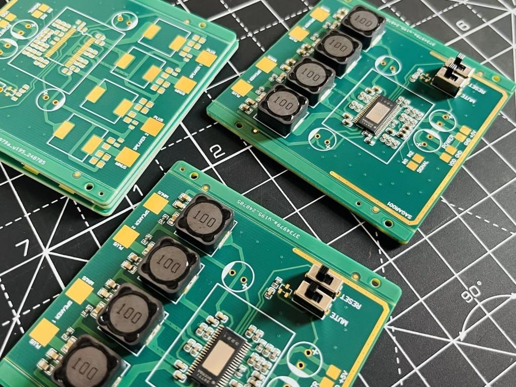
Have you ever wondered why most multilayer PCB have even more layers? The most common configurations are four, six, or eight layers. Many engineers usually choose even layers when designing multilayer PCBs because these even-numbered designs are more stable, cost-effective, and easier to manufacture. So why are even-numbered layers more stable than odd-numbered layers? Let’s find out.
Signal Integrity and Return Paths
One of the key technical drivers for even-layer Multilayer PCB designs is the necessity of clean return paths for signal integrity. High-speed signals require a dedicated ground or power layer as a reference. With even layers, designers can neatly pair every signal layer with a ground or power plane, minimising electromagnetic interference and crosstalk.
Engineers ensure a low-impedance path for return currents by aligning signal layers with reference planes. In odd-layer boards, this pairing becomes harder to maintain, leading to signal degradation and increased EMI. Hence, even-numbered configurations are favoured for applications demanding high-speed data, such as computing, telecommunications, and automotive electronics.
Manufacturing Efficiency and Cost Considerations
From a manufacturing standpoint, even-layer Multilayer PCBs are significantly easier and cheaper to produce. Laminating layers requires applying heat and pressure in a balanced manner. Manufacturers can apply uniform force with symmetrical, even-layer stacks, ensuring proper adhesion and alignment.
Odd-layer PCBs disrupt this symmetry, creating internal stress that can result in delamination or bowing. To compensate, manufacturers might add dummy layers, ironically bringing the total count back to even. This extra step adds time and cost. Therefore, choosing even layers from the start ensures quality and saves on production expenses.
Thermal and Mechanical Stability
Thermal stability is another reason designers prefer even-layer Multilayer PCB structures. During operation, electronic components generate heat. A balanced PCB dissipates this heat evenly, maintaining component performance and prolonging board life. An asymmetrical board with odd layers might exhibit uneven heat distribution, leading to hot spots and thermal stress.
Moreover, mechanical forces—such as vibration and flexing—are distributed more evenly in symmetrical boards. This stability benefits devices like smartphones, medical instruments, and aerospace systems. Even layers create a harmonised structure, reducing the risk of microcracks and other mechanical failures.
Design Tools and Industry Standards
Most PCB design software and industry guidelines are optimised for even-layer configurations. Software tools like Altium Designer, KiCAD, and Mentor Graphics offer stack-up templates that assume even layers. These templates make it easier for engineers to comply with IPC standards and ensure manufacturability.
Testing protocols and automated inspection systems are also calibrated for these common designs. An even-layer Multilayer PCB allows faster prototyping and smoother hand-offs between design and fabrication teams. The result is faster time-to-market and fewer redesigns.
Application-Specific Considerations
Different applications demand different Multilayer PCB configurations. In consumer electronics, compact designs often rely on four or six layers. In contrast, aerospace and defence systems may require ten or more layers for shielding and redundancy. Regardless of the use case, the preference for even layers remains consistent.
Engineers may sometimes need to add impedance control, shielding, or isolation layers. Even-layer stack-ups accommodate these needs more efficiently. Odd-layer solutions often struggle with these additional requirements, leading to performance compromises or redesigns.
Exceptions and Edge Cases
Although rare, odd-layer Multilayer PCBs are used in some situations. For instance, a designer might use three layers to save cost in low-frequency analogue circuits. However, the savings are often offset by added complexity in fabrication. Manufacturers may still laminate a fourth dummy layer to maintain structural balance.
Such exceptions typically occur in legacy systems or experimental designs. They are not recommended for high-speed or mission-critical applications. Sticking to even layers offers better electrical, thermal, and mechanical performance in nearly all modern use cases.
Why Even Layers Dominate Multilayer PCB Design
The dominance of even-layer configurations in Multilayer PCB design is no accident. It synthesises best practices, manufacturing realities, and long-term reliability goals for electrical engineering. From improved signal integrity to easier fabrication and thermal balance, even layers deliver on multiple fronts.
Choosing an even-layer Multilayer PCB is a strategic decision that enhances performance and reduces cost. While odd layers may appear in niche scenarios, they are the exception, not the rule. For engineers and manufacturers focused on quality, efficiency, and scalability, even-layer designs remain the gold standard in PCB development.