Interactive Tools for Heavy Copper PCB Design: Enhancing Efficiency
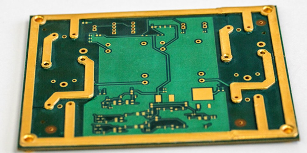
Designing Heavy Copper PCB demands precision beyond standard boards – optimizing thermal performance, current capacity, and structural integrity from the outset. While traditional PCB tools struggle with high-power requirements, modern interactive design platforms like Altium Designer and Cadence Allegro empower engineers to simulate thermal behaviour, adjust trace geometries, and validate current loads in real time. These solutions transform complex challenges – from managing 20oz copper layers to preventing thermal runaway – into visualized, data-driven decisions, significantly reducing prototyping cycles while ensuring reliability in demanding industrial applications.
Heavy Copper PCB Design Assurance: The Role of Real-Time Visualization
Interactive design tools have revolutionized visualization in PCB design. With 3d modelling and real-time rendering, engineers can inspect layers, trace paths, and component placements more intuitively. This is especially useful for heavy copper designs where space and heat are critical constraints. Seeing the effects of copper thickness on thermal dissipation or mechanical stress is a game-changer.
Furthermore, many tools now offer real-time DRC (Design Rule Check) features. These alerts flag violations immediately, allowing designers to correct errors without halting their workflow. This feedback loop is invaluable for heavy copper boards, where mistakes can lead to catastrophic thermal failures. It enhances design confidence and improves the turnaround time for production.

Thermal Management Simulations: Taming the Heat
Thermal analysis is crucial for any Heavy Copper PCB. Copper conducts heat well but can also trap and redistribute that heat unevenly in high-current scenarios. Interactive simulation tools help designers evaluate thermal load distribution before building the prototype, saving time and money.
Most high-end PCB tools now come with built-in thermal simulation features. These allow users to experiment with copper weights, trace widths, and heat sinks. Using thermal maps and heat flow analysis, engineers can predict hot spots and resolve them early in the design process. This proactive approach improves overall system stability and extends product life.
Current Carrying Capacity Calculators: Avoiding Burnout
One of the most critical aspects of designing for heavy copper is calculating how much current each trace can safely carry. Underestimating this can cause overheating, failure, and even safety hazards. Fortunately, interactive calculators embedded in most modern EDA tools enable quick and accurate trace current analysis.
Designers can enter data such as trace width, copper thickness, and temperature rise and receive immediate feedback. This information empowers them to make decisions that balance space and performance. These calculators are handy when designing complex, multilayer, heavy copper PCBS where current loads are distributed unevenly.

Design Automation: Speed Without Sacrificing Precision
Design automation is no longer a luxury; it’s necessary for complex, heavy copper PCBs projects. Automation features like auto-routing optimization and BOM generation help reduce manual errors and accelerate the time from concept to prototype.
Interactive tools now come with AI-enhanced automation. These systems learn from past designs and suggest optimal layouts and routing strategies. These intelligent suggestions can reduce EMI, improve thermal distribution, and increase reliability for high-power applications. Plus, automation allows engineers to iterate faster without compromising on design integrity.
Material Selection Assistance: Matching Design with Function
Selecting the right material is crucial in designing a Heavy Copper PCB. Not all laminates can handle increased copper weight’s mechanical and thermal stress. Many interactive tools offer material selection guides based on the intended operating environment.
For instance, if a board is intended for use in a high-temperature automotive setting, the tool might suggest polyimide over standard FR4. These software-guided recommendations simplify the decision-making process and ensure that the PCB will perform reliably under specific conditions, avoiding costly redesigns.

DFM and DFA Checks: Ready for the Real World
Designing a perfect Heavy Copper PCB layout in software is one thing; ensuring it can be manufactured is another. Design for Manufacturability (DFM) and Design for Assembly (DFA) features ensure that your design is theoretically sound and practically viable.
These interactive checks help validate spacing, hole sizes, copper clearances, and mechanical fit. They alert the designer to potential issues during fabrication or assembly. By integrating these checks into the early stages of design, engineers reduce the risk of production delays and increase first-pass yield.
Elevating Designs with Interactive Tools for Heavy Copper PCB
Heavy Copper PCB design has transcended traditional approaches in today’s power-intensive applications, becoming a sophisticated interplay of engineering expertise and advanced interactive tools. These platforms have evolved from mere drafting aids to indispensable partners – enabling real-time thermal analysis, automated optimization, and manufacturability validation that elevate design quality. As industrial demands grow more complex, leveraging these tools transforms from a convenience to a critical competitive edge, empowering engineers to confidently navigate the challenges of high-current layouts while achieving unprecedented reliability and performance benchmarks.

