
SSD PCB Trends: What the Next Generation Storage Modules Demand
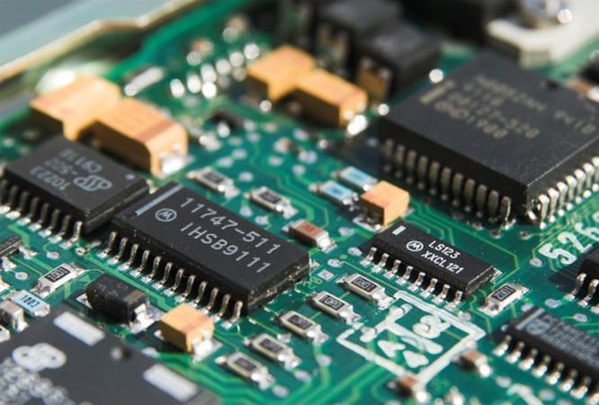
SSD PCB Trends: What the Next Generation Storage Modules Hold for the SSD Market. The SSD market is expanding rapidly as data-driven technologies dominate the global economy. From hyperscale data centers to high-end gaming laptops, every device now demands faster storage. This growth has put tremendous pressure on the SSD PCB, which serves as the backbone of every solid-state drive. As NAND flash transitions from TLC to QLC and even PLC formats, and as PCIe interfaces progress from Gen 4 to Gen 6, PCB designers must manage higher signal speeds, tighter layouts, and more complex thermal conditions. Without a capable PCB, even the best controller or NAND array cannot perform to its full potential.
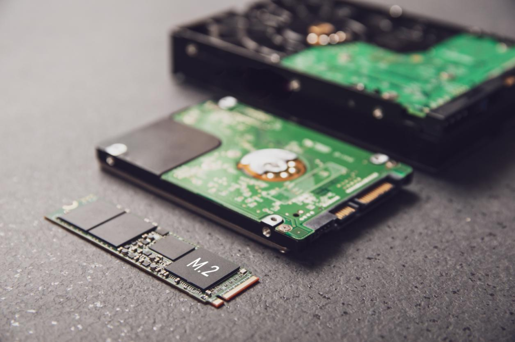
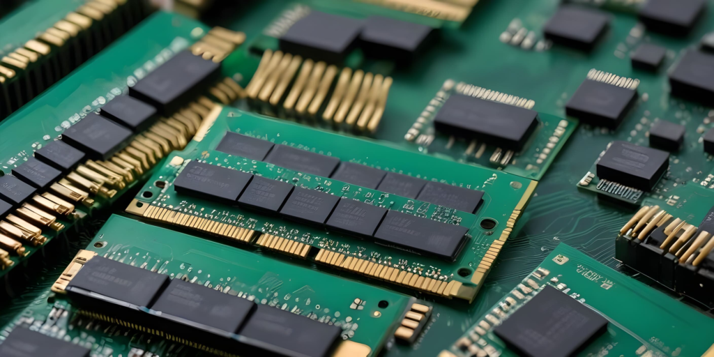
Miniaturization and Multi-Layer Design
Form factor reduction is one of the strongest SSD design trends. Whether in M.2, U.2, or EDSFF formats, space efficiency has a direct impact on thermal and power management. To achieve this, engineers now use high-density interconnect (HDI) boards with 10 to 14 layers. Blind and buried vias allow compact routing between the controller, NAND, and DRAM chips. Multi-layer stack-ups also isolate power and ground planes, improving signal clarity. In thin ultrabooks, SSD PCBs often measure under 0.8 mm in thickness, while still supporting PCIe Gen 5-level performance. This miniaturization drives the development of new testing standards and assembly automation to maintain yield consistency.
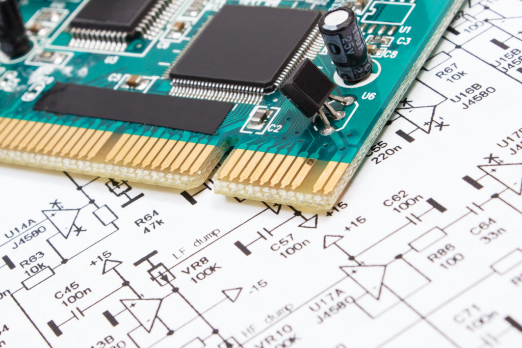
High-Speed Signal Integrity
As SSDs approach 32 GT/s and beyond, maintaining clean signal paths becomes non-negotiable. Crosstalk, skew, and impedance mismatch can degrade data integrity in nanoseconds. Engineers address these issues by utilizing controlled dielectric materials and precise routing geometry. High-frequency laminates, such as Megtron 7 and Tachyon 100G, have become preferred options for SSD PCBs fabrication due to their ultra-low dissipation factor (Df) and stable dielectric constant across various temperature ranges. At the same time, differential pair tuning and via stub removal—achieved through back-drilling—ensure that PCIe and NVMe signals maintain their eye pattern clarity. These refinements directly translate into faster boot times, better latency, and longer product lifespans.
Thermal Management and Power Efficiency
As SSD controllers now consume over 7 W of power under load, efficient heat dissipation is crucial for their operation. Copper planes, thermal vias, and embedded heat spreaders are increasingly integrated into the PCB stack-up. In enterprise systems, designers often couple PCBs with aluminum heatsinks or vapor chambers for long-term stability and reliability. The latest innovation features thermally conductive dielectric layers, which enhance heat flow while maintaining signal isolation. Furthermore, optimized power delivery networks (PDN) ensure minimal IR drop across layers, improving efficiency and reducing EMI. For consumer drives, better thermal control means sustained performance during large file transfers or gaming sessions.
Advanced Manufacturing and Automation
High-speed SSDs require precision that manual production can’t achieve. Modern factories utilize laser direct imaging, automated solder mask application, and 3D automated optical inspection (AOI) to ensure that every trace meets design intent. Robotic handling reduces contamination and misalignment, especially in fine-pitch BGA pads for NAND packages. Companies like AT&S, TTM Technologies, and Unimicron are investing in digital twins and AI-based defect detection to improve first-pass yield. These processes make SSD PCB manufacturing more scalable and consistent, aligning with the reliability standards demanded by data center OEMs.
Material Innovation and Environmental Responsibility
Performance materials dominate the current discussion, but cost and sustainability are catching up. Designers are experimenting with mixed dielectric stack-ups—using advanced laminates in high-speed layers and FR-4 in non-critical regions—to optimize budgets. Halogen-free and lead-free materials have become industry norms, complying with RoHS and REACH directives. Some SSD PCB suppliers now utilize bio-based epoxy systems, which reduce carbon emissions by up to 20% compared to conventional resins. The shift toward greener materials demonstrates that innovation can be achieved without compromising the environment.
Reliability, Testing, and Quality Control
To survive 24/7 data center operation, SSD PCBs must withstand extreme conditions. Accelerated aging, vibration, and humidity testing verify the long-term stability of the product. For example, JEDEC JESD22-A104 defines a temperature cycling range from -55 °C to +125 °C to simulate years of real-world use. Boards are also subjected to IPC-6016 Class 3 standards, ensuring they meet the highest reliability for critical electronics. Solder joint reliability remains a top concern, especially in thin PCBs exposed to repeated thermal expansion. Continuous monitoring of reflow profiles and cross-sectional analysis helps manufacturers identify and eliminate potential weak points before mass production begins.
The Future of SSD PCB Design
As data moves closer to the edge, the SSD PCB will continue to evolve as a high-speed, thermally stable foundation for next-generation storage. Expect tighter integration with chiplet architectures, 3D stacking, and embedded passive components. Flexible PCBs and hybrid rigid-flex configurations may soon power ultra-thin portable SSDs. Looking forward, AI-assisted design tools will predict signal behavior before fabrication, cutting development time and cost. Ultimately, the performance leap of tomorrow’s SSDs will depend not only on NAND or controller innovation but on the sophistication of the PCB that ties them together. The board beneath the silicon will remain the silent enabler of every byte stored and retrieved at lightning speed.